PI74ALVCH16271 데이터 시트보기 (PDF) - Pericom Semiconductor
부품명
상세내역
일치하는 목록
PI74ALVCH16271 Datasheet PDF : 6 Pages
| |||
PI74ALVCH16271
1122334455667788990011223344556677889900112233445566778899001122112233445566778899001122334455667788990011122233-44B5566i77t8899T0011o221122233444-55B6677i88t9900M112233u4455l66t77ip8899l00e11x2233e44d556677B8899u0011s2211E2233x44c5566h7788a99n0011g22e3344r5566w7788i99t00h112233344-55S6677t88a9900t11e2211O2233u4455t66p7788u99t0011s22
Maximum Ratings
(Above which the useful life may be impaired. For user guidelines, not tested.)
Storage Temperature .................................................. 65°C to +150°C
Supply Voltage Range, VCC ........................................... 0.5V to 4.6V
Input Voltage Range,VI :
Except I/O ports (See Note 1): ........................................ 0.5V to 4.6V
I/O ports (See Notes 1 and 2) .............................. 0.5V to VCC + 0.5V
Output Voltage Range, VO (See Notes 1and 2) .. 0.5V to VCC + 0.5V
Input Clamp current, IIK (VI < 0) .............................................. 50mA
Output Clamp current, IOK (VO < 0 or VO > VCC) ................... ±50mA
Continous Output Current, IO (VO = 0 to VCC) ........................ ±50mA
Continous Current through each VCC or GND ........................ ±100mA
Maximum Power Dissipation:
A package ................................................................... 1W
V package ................................................................ 1.4W
Note:
Stresses greater than those listed under MAXIMUM
RATINGS may cause permanent damage to the device.
This is a stress rating only and functional operation of the
device at these or any other conditions above those
indicated in the operational sections of this specification
is not implied. Exposure to absolute maximum rating
conditions for extended periods may affect reliability.
Notes:
1. The input and output negative-voltage ratings maybe exceeded if the input
and outputclamp-current ratings are observed.
2. This value is limited to 4.6V maximum.
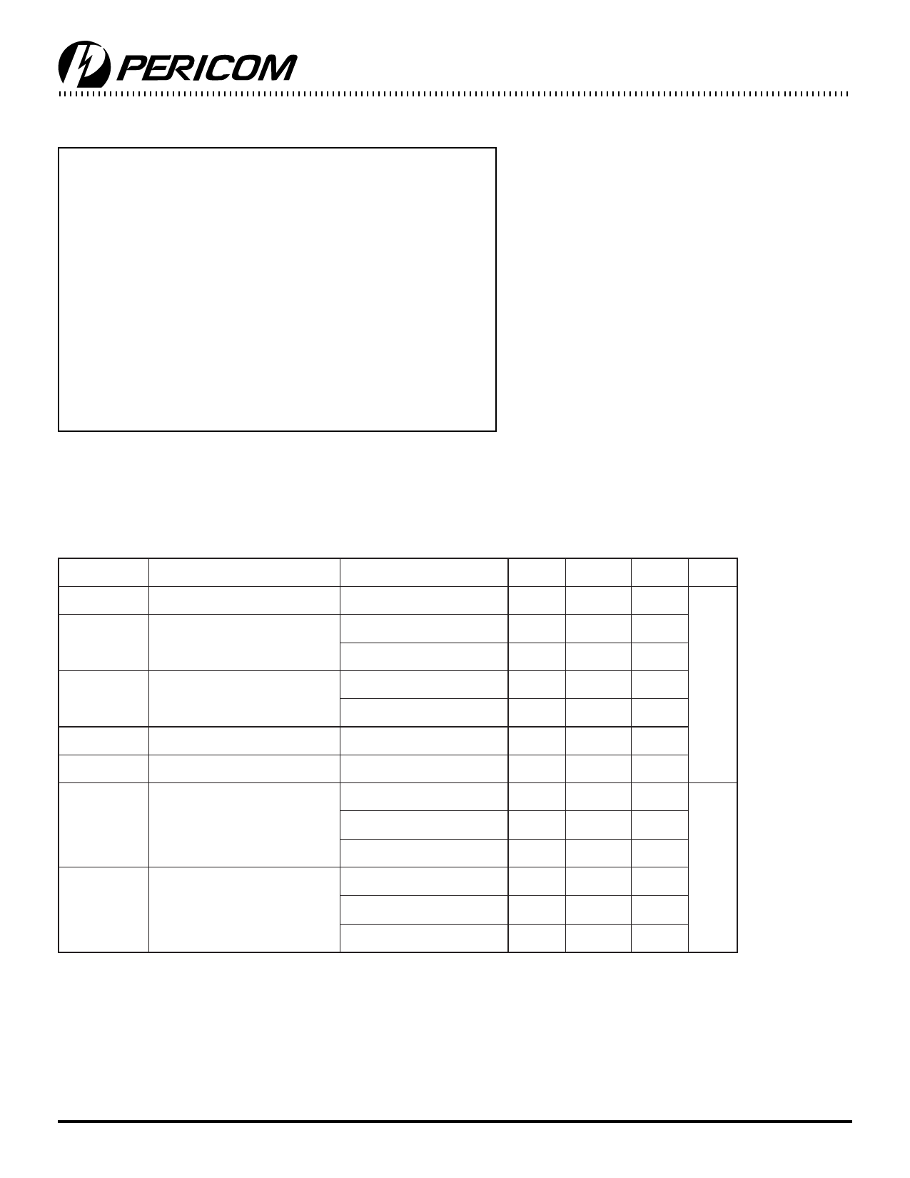
DC Electrical Characteristics (Over the Operating Range, TA = –40°C to +85°C, VCC = 3.3V ± 10%)
Parameters
Description
Test Conditions(3)
Min. Typ. Max. Units
VCC
Supply Voltage
2.3
3.6
VIH
Input HIGH Voltage
VCC = 2.3V to 2.7V
1.7
VCC = 2.7V to 3.6V
2.0
VIL
Input LOW Voltage
VCC = 2.3V to 2.7V
VCC = 2.7V to 3.6V
0.7
V
0.8
VIN
Input Voltage
0
VCC
VOUT Output Voltage
0
VCC
VCC = 2.3V
-12
IOH
HIGH-level Output Current
VCC = 2.7V
-12
VCC = 3.0V
VCC = 2.3V
-24
mA
12
IOL
LOW-level Output Current
VCC = 2.7V
12
VCC = 3.0V
24
Note:
3. Unused control inputs must be held HIGH or LOW to prevent them from floating.
3
PS8360 02/02/99
Share Link: 