PI74ALVCH162268A 데이터 시트보기 (PDF) - Pericom Semiconductor
부품명
상세내역
일치하는 목록
PI74ALVCH162268A Datasheet PDF : 6 Pages
| |||
PI74ALVCH162268 1122334455667788990011223344556677889900112233445566778899001122112233445566778899001122334455667788990011223344556677889900112211223344556677889900112233445566778899001122334455667788990011221122334455667788990011223344556677889900112233445566778899001122112233445566778899001122
12-Bit To 24-Bit Registered Bus Exchanger
with 3-State Outputs
Product Features
• PI74ALVCH162268 is designed for low voltage operation
VCC = 2.3V to 3.6V
• Hysteresis on all inputs
• Typical VOLP (Output Ground Bounce)
< 0.8V at VCC = 3.3V, TA = 25°C
• Typical VOHV (Output VOH Undershoot)
< 2.0V at VCC = 3.3V, TA = 25°C
• B-port outputs have equivalent 26Ω series resistors,
no external resistors are required.
• Bus Hold retains last active bus state during 3-state
eliminates the need for external pullup resistors
• Industrial operation at –40°C to +85°C
• Packages available:
– 56-pin 240 mil wide plastic TSSOP (A56)
– 56-pin 300 mil wide plastic SSOP (V56)
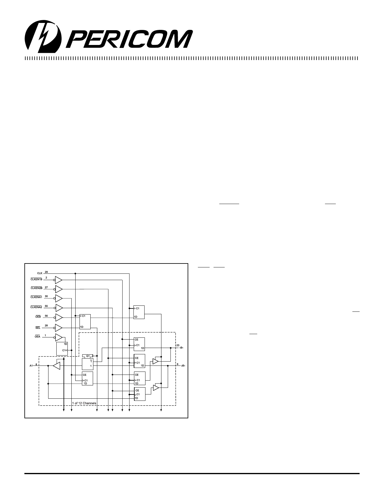
Logic Block Diagram
Product Description
Pericom Semiconductor’s PI74ALVCH series of logic circuits are
produced in the Company’s advanced 0.5 micron CMOS
technology, achieving industry leading speed.
This 12-bit to 24-bit registered bus exchanger is designed for 2.3V
to 3.6V Vcc operation.
The PI74ALVCH162268 is used for applications in which data
must be transferred from a narrow high-speed bus to a wide, lower
frequency bus.
The device provides synchronous data exchange between the two
ports. Data is stored in the internal registers on the low-to-high
transition of the clock (CLK) input when the appropriate clock
enable (CLKEN) inputs are low. The select (SEL) line is
synchronous with CLK and selects 1B or 2B input data for the A
outputs.
For data transfer in the A-to-B direction, a two stage pipeline is
provided in the A-to-1B path, with a single storage register in the
A-to-2B path. Proper control of these inputs allows two sequential
12-bit words to be presented synchronously as a 24-bit word on the
B-port. Data flow is controlled by the active-low output enables
(OEA, OEB). These control terminals are registered so bus direction
changes are synchronous with CLK.
The B outputs, which are designed to sink up to 12mA, include
equivalent 26Ω resistors to reduce overshoot and undershoot.
To ensure the high-impedance state during power up or power
down, a clock pulse should be applied as soon as possible and OE
should be tied to VCC through a pullup resistor, the minimum value
of the resistor is determined by the current-sinking capability of
the driver. Because OE is being routed through a register, the
active state of the outputs cannot be determined prior to the arrival
of the first clock pulse.
Active bus-hold circuitry is provided to hold unused or floating
data inputs at a valid logic level.
1
PS8352 11/04/98
Share Link: 