SL74HC597 데이터 시트보기 (PDF) - System Logic Semiconductor
부품명
상세내역
일치하는 목록
SL74HC597
System Logic Semiconductor

SL74HC597 Datasheet PDF : 9 Pages
| |||
SL74HC597
Operation
Reset shift register
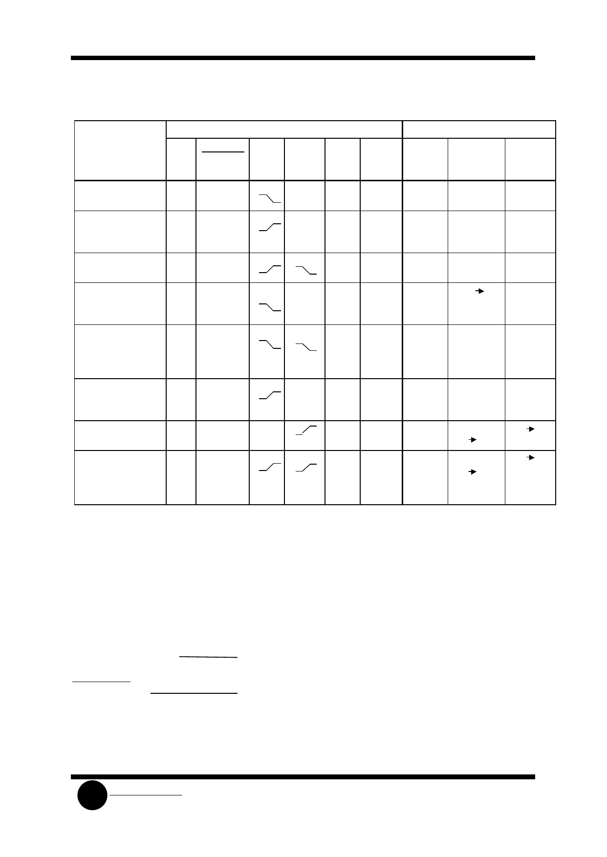
FUNCTION TABLE
Inputs
Resulting Function
Reset SerialShift/ Latch
ParallelLoad Clock
L
X
L,H,
Shift
Clock
X
Serial
Input
SA
X
Parallel Latch
Inputs Contents
A-H
X
U
Shift
Register
Contents
L
Output QH
L
Reset shift register; L
X
load parallel data
into data latch
Load parallel data
H
H
into data latch
Transfer latch
H
L
contents to shift
register
Contents of data
H
H
latch and shift
register are
unchanged
Load parallel data
H
L
into data latch and
shift register
Shift serial data into H
H
shift register
Load parallel data
H
H
into data latch and
shift serial data into
shift register
SR = shift register contents
LR = latch register contents
D = data (L,H) at serial data input SA
U = remains unchanged
X
X
a-h
a-h
L
L
L,H, X
a-h
a-h
U
U
L,H, X
X
X
U
LRN SRN
LRH
L,H, L,H, X
X
U
U
U
X
X
a-h
a-h
a-h
h
X
D
X
*
SRA=D; SRG SRH
SRN SRN+1
D
a-h
a-h
SRA=D; SRG SRH
SRN SRN+1
X = don’t care
a-h = data at parallel data inputs A-H
* = depends on Latch Clock input
INPUTS:
A, B, C, D, E, F, G, H - Parallel data inputs. Data on
these inputs is stored in the input latch on the rising
edge of the Latch Clock input.
SA - Serial data input. Data on this input is shifted into
the shift register on the rising edge of the Shift Clock
input if Serial Shift/Parallel Load is high. Data on this
input is ignored when Serial Shift/
Parallel Load is low.
SERIAL SHIFT/PARALLEL LOAD - Shift register
mode control. When a high level is applied to this pin,
the shift register is allowed to serially shift data. When
a low level is applied to this pin, the shift register
accepts parallel data from the input latch, and serial
shifting is inhibited.
RESET - Asynchronous, Active-low shift register
reset. A low level applied to this input resets the shift
register to a low level, but does not change the data in
the input latch.
SHIFT CLOCK - Serial shift register clock. A low-to-
high transition on this input shifts data on the Serial
Data Input into the shift register and data in stage H is
shifted out QH, being replaced by the data previously
stored in stage G.
LATCH CLOCK - A low-to-high transition on this
input loads the parallel data on inputs A-H into the
input latch.
OUTPUT:
QH - Serial data output. This pin is the output from the
last stage of the shift register.
SLS
System Logic
Semiconductor
Share Link: