A6275EA 데이터 시트보기 (PDF) - Allegro MicroSystems
부품명
상세내역
일치하는 목록
A6275EA Datasheet PDF : 12 Pages
| |||
A6275
Serial-Input Constant-Current Latched LED Driver
with Open LED Detection and Dot Correction
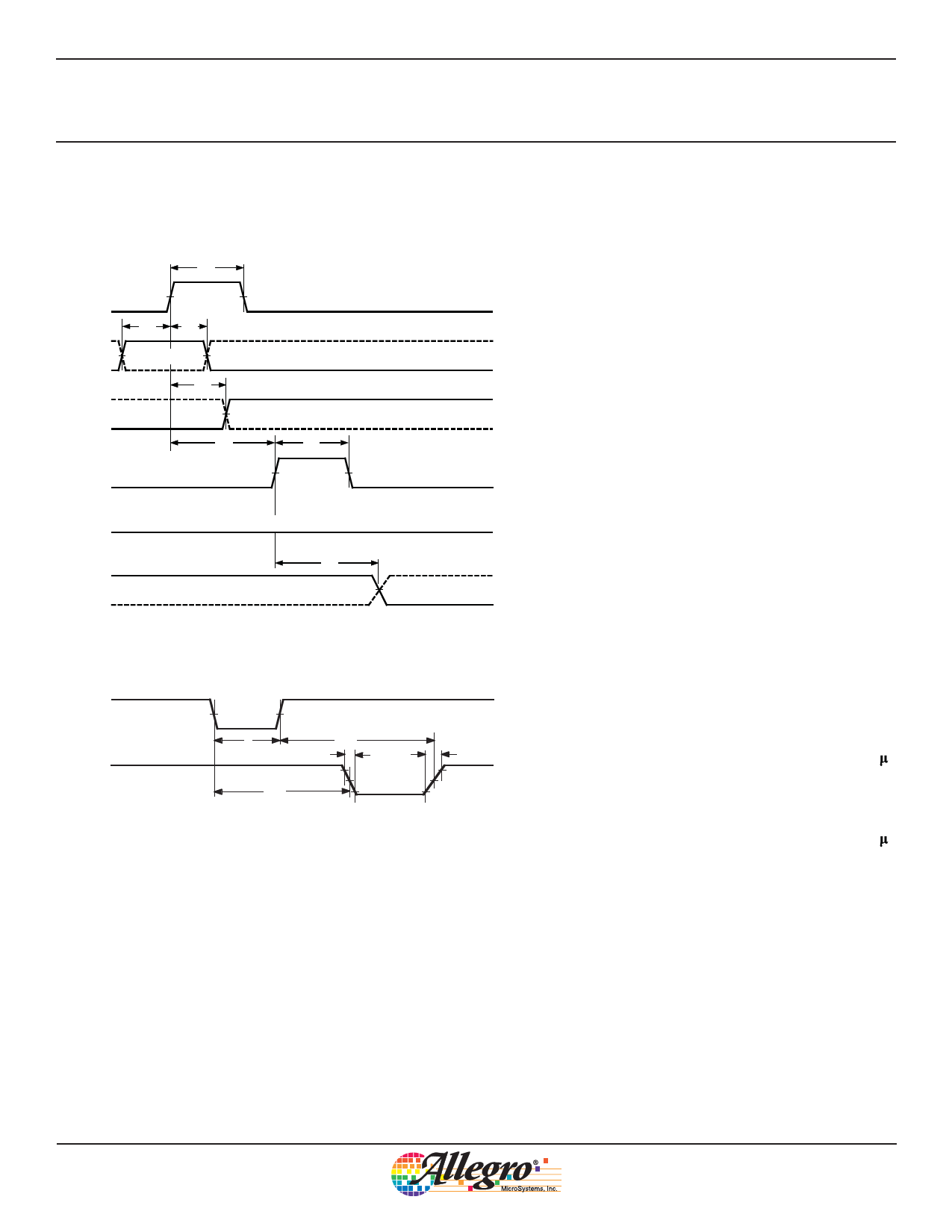
CLOCK
SERIAL
DATA IN
SERIAL
DATA OUT
LATCH
ENABLE
TIMING REQUIREMENTS and SPECIFICATIONS
(Logic Levels are VDD and Ground)
C
50%
A
B
DATA
50%
tp
50%
DATA
D
E
50%
OUTPUT
ENABLE
LOW = ALL OUTPUTS ENABLED
OUT N
OUTPUT
ENABLE
OUT N
tp
HIGH = OUTPUT OFF
50%
DATA
LOW = OUTPUT ON
Dwg. WP-029-1
HIGH = ALL OUTPUTS DISABLED (BLANKED)
50%
F
t pHL
t pLH
90%
tf
tr
DATA
50%
10%
Dwg. WP-030-1A
A. Data Active Time Before Clock Pulse
(Data Set-Up Time), tsu(D) ............................. 50 ns
B. Data Active Time After Clock Pulse
(Data Hold Time), th(D) ................................. 20 ns
C. Clock Pulse Width, tw(CK) .................................. 50 ns
D. Time Between Clock Activation
and Latch Enable, tsu(L) ............................... 100 ns
E. Latch Enable Pulse Width, tw(L) ...................... 100 ns
F. Output Enable Pulse Width, tw(OE) ................... 4.5 s
NOTE: Timing is representative of a 10 MHz clock. Sig-
nificantly higher speeds are attainable.
Max. Clock Transition Time, tr or tf ....................... 10 s
Serial data present at the input is transferred to the shift
register on the logic 0-to-logic 1 transition of the CLOCK input
pulse. On succeeding CLOCK pulses, the registers shift data in-
formation towards the SERIAL DATA OUTPUT. The serial data
must appear at the input prior to the rising edge of the CLOCK
input waveform.
Information present at any register is transferred to the
respective latch when the LATCH ENABLE is high (serial-to-
parallel conversion). The latches continue to accept new data as
long as the LATCH ENABLE is held high. Applications where
the latches are bypassed (LATCH ENABLE tied high) will
require that the OUTPUT ENABLE input be high during serial
data entry.
When the OUTPUT ENABLE input is high, the output sink
drivers are disabled (OFF). The information stored in the latches
is not affected by the OUTPUT ENABLE input. With the OUT-
PUT ENABLE input low, the outputs are controlled by the state
of their respective latches.
Allegro MicroSystems, Inc.
6
115 Northeast Cutoff
Worcester, Massachusetts 01615-0036 U.S.A.
1.508.853.5000; www.allegromicro.com
Share Link: 