W83194R-39A 데이터 시트보기 (PDF) - Winbond
부품명
상세내역
일치하는 목록
W83194R-39A Datasheet PDF : 21 Pages
| |||
W83194R-39/-39A
Bytes sequence order for I2C controller :
PRELIMINARY
Clock Address
A(6:0) & R/W
Ack
8 bits dummy
Command code
Ack
8 bits dummy
Byte count
Ack
Byte0,1,2...
until Stop
Set R/W to 1 when “read back”, the data sequence is as follows :
Clock Address
A(6:0) & R/W
Ack
Byte 0
Ack
Byte 1
Ack
Byte2, 3, 4...
until Stop
8.3 SERIAL CONTROL REGISTERS
The Pin column lists the affected pin number and the @PowerUp column gives the default state at
true power up. "Command Code" byte and "Byte Count" byte must be sent following the
acknowledge of the Address Byte. Although the data (bits) in these two bytes are considered "don't
care", they must be sent and will be acknowledge. After that, the below described sequence
(Register 0, Register 1, Register 2, ....) will be valid and acknowledged.
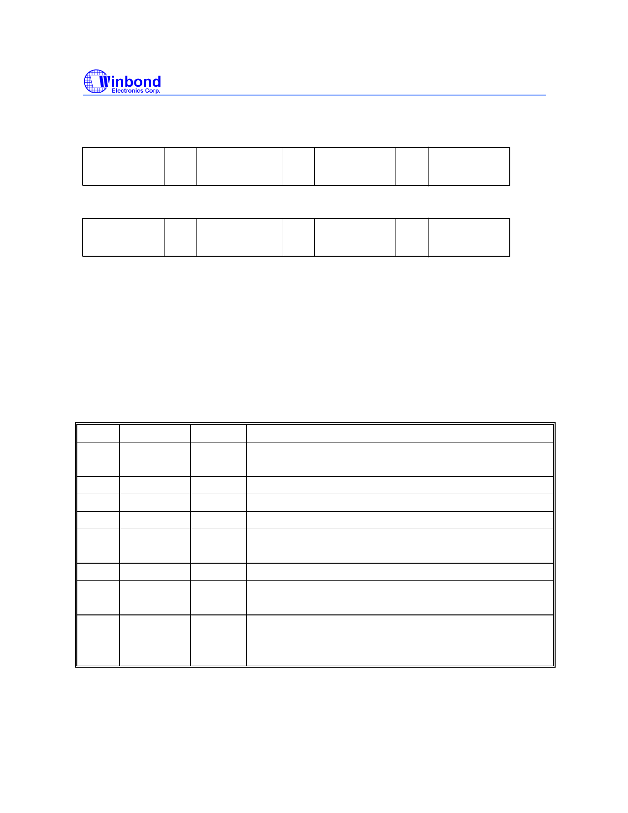
8.3.1 Register 0: CPU Frequency Select Register (default = 0)
Bit @PowerUp
7
0
6
0
5
0
4
0
3
0
2
0
1
0
0
0
Pin
Description
-
0 = ¡Ó0.25% Spread Spectrum Modulation
1 = ¡Ó0.5% Spread Spectrum Modulation
-
SSEL2 (for frequency table selection by software via I2C)
-
SSEL1 (for frequency table selection by software via I2C)
-
SSEL0 (for frequency table selection by software via I2C)
-
0 = Selection by hardware
1 = Selection by software I2C - Bit 6:4
-
SSEL3 (for frequency table selection by software via I2C)
-
0 = Normal
1 = Spread Spectrum enabled
-
0 = Running
1 = Tristate all outputs
Note : The frequency table selected by software via I2C is the same as the hardware setting
frequency table.
Publication Release Date: May 1998
-9-
Revision 0.20
Share Link: 