PDI1394L21 데이터 시트보기 (PDF) - Philips Electronics
부품명
상세내역
일치하는 목록
PDI1394L21 Datasheet PDF : 52 Pages
| |||
Philips Semiconductors
1394 full duplex AV link layer controller
Preliminary specification
PDI1394L21
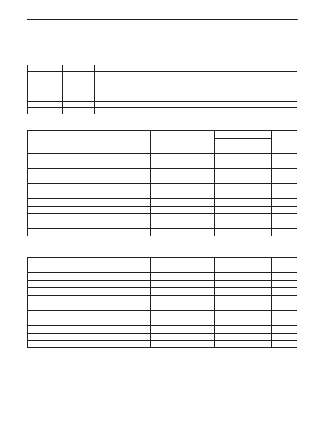
9.5 Other Pins
PIN No.
PIN SYMBOL I/O
NAME AND FUNCTION
65, 66, 67
RESERVED
NA
These pins are reserved for factory testing. For normal operation they should be connected to
ground.
51, 62, 100
N/C
NA These pins should not be connected or terminated.
30
CYCLEIN
I
Provides the capability to supply an external cycle timer signal for the beginning of 1394 bus
cycles.
33
CYCLEOUT O Reproduces the 8kHz cycle clock of the cycle master.
11
CLK25
O Auxiliary clock, value is SCLK/2 (usually 24.576 MHz)
10.0 RECOMMENDED OPERATING CONDITIONS
SYMBOL
PARAMETER
VCC
VI
VIH
VIL
IOH
IOL
dT/dV
Tamb
SCLK
AVCLK
tr
tf
DC supply voltage
Input voltage
High-level input voltage
Low-level input voltage
High-level output current
Low-level output current
Input transition rise or fall time
Operating ambient temperature range
System clock
AV interface clock
Input rise time
input fall time
CONDITIONS
LIMITS
MIN.
MAX.
3.0
3.6
0
5
2.0
0.8
8
–8
0
20
0
+70
49.147
49.157
0
24
10
10
UNIT
V
V
V
V
mA
mA
ns/V
°C
MHz
MHz
ns
ns
11.0 ABSOLUTE MAXIMUM RATINGS1, 2
In accordance with the Absolute Maximum Rating System (IEC 134). Voltages are referenced to GND (ground = 0V).
SYMBOL
PARAMETER
CONDITIONS
LIMITS
MIN
MAX
UNIT
VDD
DC supply voltage
–0.5
+4.6
V
IIK
DC input diode current
–
–50
mA
VI
DC input voltage
–0.5
+5.5
V
IOK
DC output diode current
–
±50
mA
VO
DC output voltage
–0.5
VDD +0.5
V
IO
DC output source or sink current
–
±50
mA
IGND, ICC DC VCC or GND current
–
±150
mA
Tstg
Storage temperature range
–60
150
°C
Tamb
Operating ambient temperature
0
70
°C
Ptot
Power dissipation per package
0.6
W
NOTES:
1. Stresses beyond those listed may cause permanent damage to the device. These are stress ratings only and functional operation of the
device at these or any other conditions beyond those indicated under “recommended operating conditions” is not implied. Exposure to
absolute-maximum-rated conditions for extended periods may affect device reliability.
2. The performance capability of a high-performance integrated circuit in conjunction with its thermal environment can create junction
temperatures which are detrimental to reliability. The maximum junction temperature of this integrated circuit should not exceed 150°C.
1999 Aug 06
8
Share Link: 