PCA9544A 데이터 시트보기 (PDF) - Philips Electronics
부품명
상세내역
일치하는 목록
PCA9544A Datasheet PDF : 18 Pages
| |||
Philips Semiconductors
4-channel I2C multiplexer with interrupt logic
Product data sheet
PCA9544A
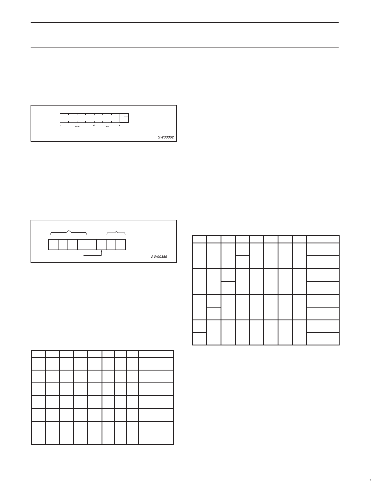
DEVICE ADDRESSING
Following a START condition the bus master must output the
address of the slave it is accessing. The address of the PCA9544A
is shown in Figure 4. To conserve power, no internal pull-up
resistors are incorporated on the hardware selectable address pins
and they must be pulled HIGH or LOW.
1 1 1 0 A2 A1 A0 R/W
FIXED
HARDWARE SELECTABLE
SW00862
Figure 4. Slave address
The last bit of the slave address defines the operation to be
performed. When set to logic 1, a read is selected while a logic 0
selects a write operation.
CONTROL REGISTER
Following the successful acknowledgement of the slave address,
the bus master will send a byte to the PCA9544A which will be
stored in the Control Register. If multiple bytes are received by the
PCA9544A, it will save the last byte received. This register can be
written and read via the I2C-bus.
INTERRUPT BITS
(READ ONLY)
CHANNEL SELECTION BITS
(READ/WRITE)
7 6 5 43 2 1 0
INT3 INT2 INT1 INT0 X B2 B1 B0
ENABLE BIT
SW00386
Figure 5. Control register
CONTROL REGISTER DEFINITION
A SCx/SDx downstream pair, or channel, is selected by the contents
of the control register. This register is written after the PCA9544A
has been addressed. The 3 LSBs of the control byte are used to
determine which channel is to be selected. When a channel is
selected, it will become active after a stop condition has been placed
on the I2C-bus. This ensures that all SCx/SDx lines will be in a
HIGH state when the channel is made active, so that no false
conditions are generated at the time of connection.
Table 1. Control Register; Write — Channel Selection/
Read — Channel Status
INT3 INT2 INT1 INT0 D3 B2 B1 B0 COMMAND
X X X X X 0 X X No channel
selected
X X X X X 1 0 0 Channel 0
enabled
X X X X X 1 0 1 Channel 1
enabled
X X X X X 1 1 0 Channel 2
enabled
X X X X X 1 1 1 Channel 3
enabled
0 0 0 0 0 0 0 0 No channel
selected;
power-up
default state
INTERRUPT HANDLING
The PCA9544A provides 4 interrupt inputs, one for each channel
and one open drain interrupt output. When an interrupt is generated by
any device, it will be detected by the PCA9544A and the interrupt
output will be driven LOW. The channel need not be active for
detection of the interrupt. A bit is also set in the control byte.
Bits 4 – 7 of the control byte correspond to channels 0 – 3 of the
PCA9544A, respectively. Therefore, if an interrupt is generated by
any device connected to channel 2, the state of the interrupt inputs is
loaded into the control register when a read is accomplished.
Likewise, an interrupt on any device connected to channel 0 would
cause bit 4 of the control register to be set on the read. The master
can then address the PCA9544A and read the contents of the
control byte to determine which channel contains the device
generating the interrupt. The master can then reconfigure the
PCA9544A to select this channel, and locate the device generating
the interrupt and clear it. The interrupt clears when the device
originating the interrupt clears.
It should be noted that more than one device can be providing an
interrupt on a channel, so it is up to the master to ensure that all
devices on a channel are interrogated for an interrupt.
The interrupt inputs may be used as general purpose inputs if the
interrupt function is not required.
If unused, interrupt input(s) must be connected to VDD through a
pull-up resistor.
Table 2. Control Register Read — Interrupt
INT3 INT2 INT1 INT0 D3 B2 B1 B0 COMMAND
0
No interrupt
on channel 0
X
X
X
X
X
X
X
1
Interrupt on
channel 0
0
No interrupt
on channel 1
X
X
X
X
X
X
X
1
Interrupt on
channel 1
0
No interrupt
on channel 2
X
X
X
X
X
X
X
1
Interrupt on
channel 2
0
No interrupt
on channel 3
X
X
X
X
X
X
X
1
Interrupt on
channel 3
NOTE: Several interrupts can be active at the same time.
Ex: INT3 = 0, INT2 = 1, INT1 = 1, INT0 = 0, means that there is no
interrupt on channels 0 and 3, and there is interrupt on channels 1
and 2.
POWER-ON RESET
When power is applied to VDD, an internal Power On Reset holds
the PCA9544A in a reset condition until VDD has reached VPOR. At
this point, the reset condition is released and the PCA9544A
registers and I2C state machine are initialized to their default states,
all zeroes causing all the channels to be deselected. Thereafter,
VDD must be lowered below 0.2 V to reset the device.
2004 Sep 29
5
Share Link: 