PCA9543A 데이터 시트보기 (PDF) - Philips Electronics
부품명
상세내역
일치하는 목록
PCA9543A Datasheet PDF : 24 Pages
| |||
Philips Semiconductors
PCA9543A
2-channel I2C switch with interrupt logic and reset
7. Functional description
Refer to Figure 1 “Block diagram of PCA9543A” on page 3.
7.1 Device address
Following a START condition, the bus master must output the address of the slave it is
accessing. The address of the PCA9543A is shown in Figure 4. To conserve power, no
internal pull-up resistors are incorporated on the hardware selectable address pins and
they must be pulled HIGH or LOW.
1 1 1 0 0 A1 A0 R/W
fixed
hardware
selectable
002aab169
Fig 4. Slave address
The last bit of the slave address defines the operation to be performed. When set to
logic 1 a read is selected, while a logic 0 selects a write operation.
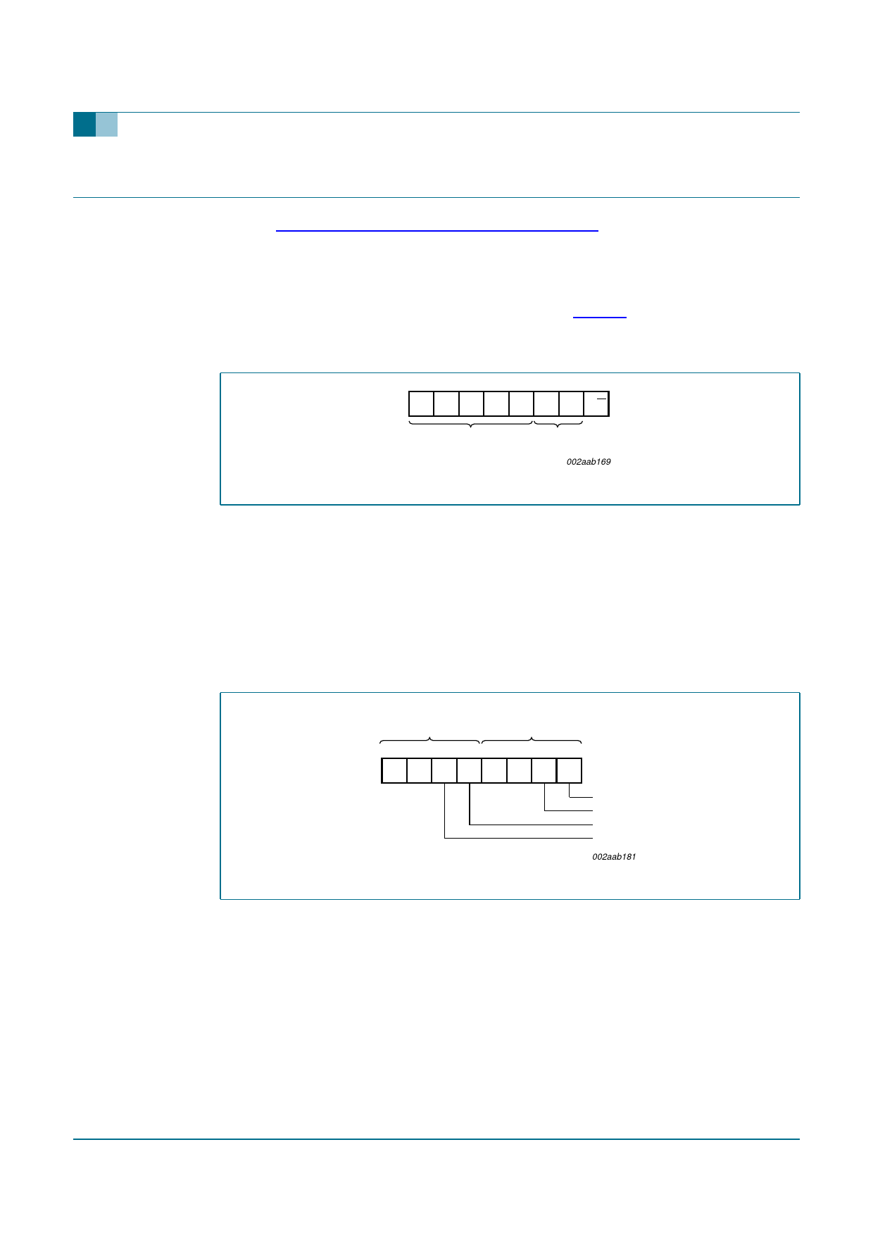
7.2 Control register
Following the successful acknowledgement of the slave address, the bus master will send
a byte to the PCA9543A, which will be stored in the control register. If multiple bytes are
received by the PCA9543A, it will save the last byte received. This register can be written
and read via the I2C-bus.
interrupt bits
(read only)
channel selection bits
(read/write)
76543210
X
X
INT INT
10
X
X B1 B0
channel 0
channel 1
INT0
INT1
002aab181
Fig 5. Control register
7.2.1 Control register definition
One or several SCx/SDx downstream pair, or channel, is selected by the contents of the
control register. This register is written after the PCA9543A has been addressed. The
2 LSBs of the control byte are used to determine which channel is to be selected. When a
channel is selected, the channel will become active after a STOP condition has been
placed on the I2C-bus. This ensures that all SCx/SDx lines will be in a HIGH state when
the channel is made active, so that no false conditions are generated at the time of
connection.
9397 750 14316
Product data sheet
Rev. 03 — 21 March 2005
© Koninklijke Philips Electronics N.V. 2005. All rights reserved.
5 of 24
Share Link: 