P4C189 데이터 시트보기 (PDF) - Semiconductor Corporation
부품명
상세내역
일치하는 목록
P4C189 Datasheet PDF : 8 Pages
| |||
P4C189
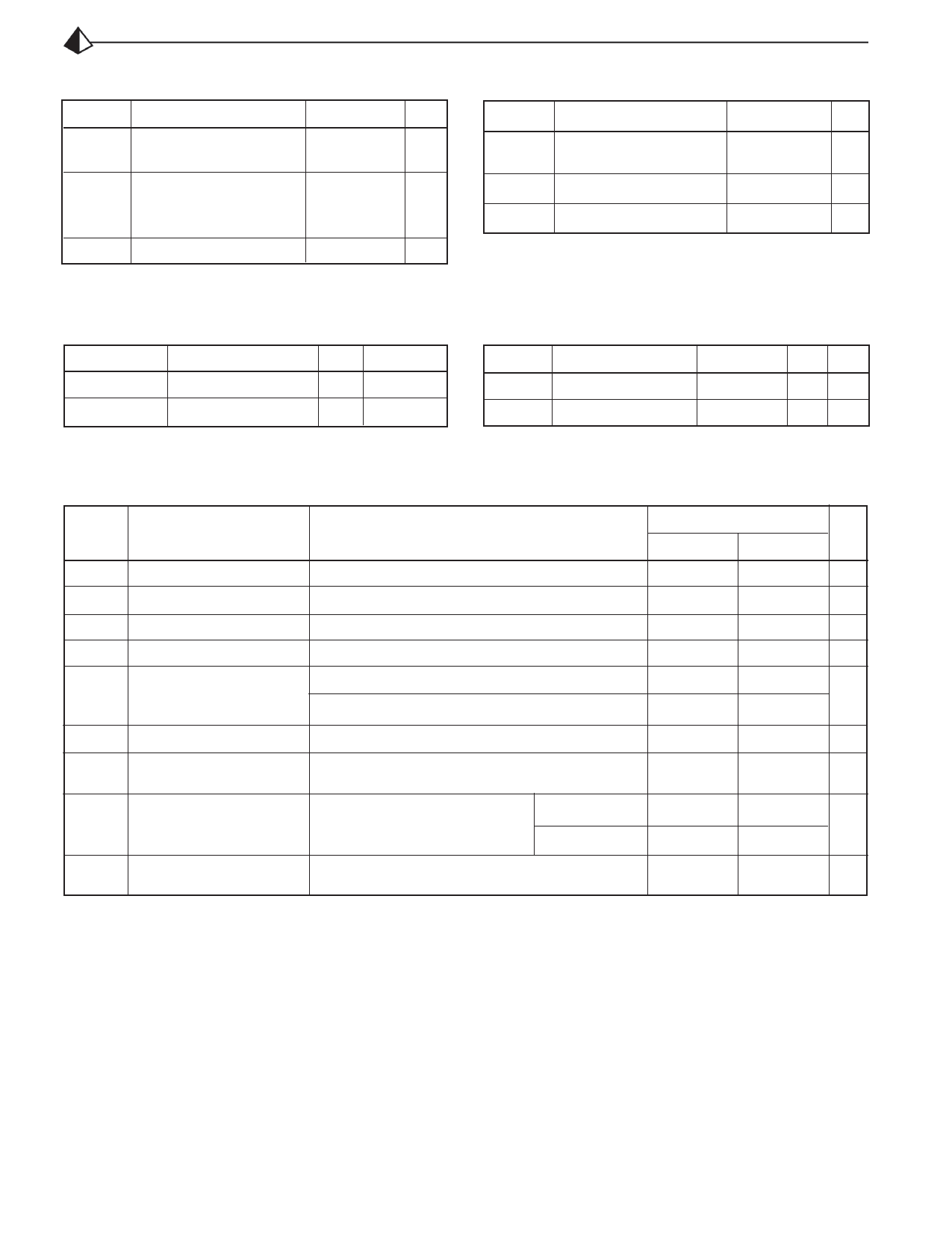
MAXIMUM RATINGS(1)
Symbol
Parameter
Value Unit
VCC
Power Supply Pin with – 0.5 to +7 V
Respect to GND
VTERM
Terminal Voltage with
Respect to GND
(up to 7.0V)
– 0.5 to
VCC +0.5
V
TA
Operating Temperature – 55 to +125 °C
Symbol Parameter
TBIAS
Temperature Under
Bias
TSTG
Storage Temperature
IOUT
DC Output Current
Value Unit
– 55 to +125 °C
– 65 to +150 °C
20
mA
RECOMMENDED OPERATING CONDITIONS
Grade(2)
Commercial
Industrial
Ambient Temp
0°C to 70°C
–40°C to 85°C
Gnd Vcc
0V 5.0V ±10%
0V 5.0V ±10%
CAPACITANCES(4)
(V = 5.0V, T = 25°C, f = 1.0MHz)
CC
A
Symbol Parameter Conditions Typ. Unit
CIN
COUT
Input Capacitance VIN = 0V
Output Capacitance VOUT = 0V
5 pF
7 pF
DC ELECTRICAL CHARACTERISTICS
Over recommended operating temperature and supply voltage(2)
Symbol
Parameter
Test Conditions
VOH Output High Voltage
V
OL
Output Low Voltage
VIH Input High Level
VIL Input Low Level
I
IL
Input Low Current
IIH Input High Current
ISC
Output Short Circuit
Current
VCC = Min., VIN = VIH or VIL, IOH = –3.0 mA
VCC = Min., VIN = VIH or VIL, IOL = 24 mA
VIN = 0.5 V (except CS)
VIN = 0.5 V (CS)
VCC = Max, VIN = 2.7V
VCC = Max., VOUT = 0.0V
ICC Power Supply Current VCC = Max.
Commercial
Industrial
IL
Output Leakage Current VOUT = VCC, VCC = Max.
P4C189
Unit
Min.
Max.
2.4
V
0.5
V
2.0
V
0.8
V
-0.6
mA
-1.2
5
µA
-150
-60
mA
55
mA
70
50
µA
Notes:
1. Stresses greater than those listed under MAXIMUM RATINGS may
cause permanent damage to the device. This is a stress rating only
and functional operation of the device at these or any other conditions
above those indicated in the operational sections of this specification
is not implied. Exposure to MAXIMUM rating conditions for extended
periods may affect reliability.
2. Extended temperature operation guaranteed with 400 linear feet per
minute of air flow.
3. Transient inputs with VIL and IIL not more negative than –3.0V and
–100mA, respectively, are permissible for pulse widths up to 20 ns.
4. This parameter is sampled and not 100% tested.
5. CE is LOW and WE is HIGH for READ cycle.
6. WE is HIGH, and address must be valid prior to or coincident with CE
transition LOW.
7. Transition is measured ±200mV from steady state voltage prior to
change with specified loading in Figure 1. This parameter is sampled
and not 100% tested.
8. Read Cycle Time is measured from the last valid address to the first
transitioning address.
Document # SRAM100 Rev OR
Page 2 of 8
Share Link: 