NTE935 데이터 시트보기 (PDF) - NTE Electronics
부품명
상세내역
일치하는 목록
NTE935
NTE Electronics

NTE935 Datasheet PDF : 2 Pages
| |||
Electrical Characteristics: (+25°C ≤ TJ ≤ +150°C, VIN –VOUT = 5V and IOUT = 2.5A, Note 1
unless otherwise specified)
Parameter
Test Conditions
Line Regulation
Load Regulation
Thermal Regulation
Adjustment Pin Current
3V ≤ (VIN –VOUT) ≤ 35V, IL = 0.01A, Note 2
3V ≤ (VIN –VOUT) ≤ 35V, IL = 0.01A, TA = +25°C, Note 2
10mA ≤ IOUT ≤ 5A, Note 2
10mA ≤ IOUT ≤ 5A, TA = +25°C, Note 2
Pulse = 20ms, TJ = +25°C
Adjustment Pin Current Change 10mA ≤ IL ≤ 5A, 3V ≤ (VIN – VOUT) ≤ 35V
Reference Voltage
3 ≤ (VIN – VOUT) ≤ 35V, 10mA ≤ IOUT ≤ 5A, P ≤ 50W,
Note 3
Temperature Stability
TMIN ≤ TJ ≤ TMAX
Minimum Load Current
(VIN –VOUT) = 35V
Current Limit
(VIN – VOUT) ≤10V
(VIN – VOUT) ≤ 30V
RMS Output Noise, % of VOUT TJ = +25°C, 10Hz ≤ f ≤ 10kHz
Ripple Rejection Ratio
VOUT= 10V, f = 120Hz
CADJ = 10µF
Long Term Stability
TJ = +125°C
Min Typ Max Unit
– 0.02 0.06 %/V
– 0.005 0.03 %/V
– 0.3 1.0 %
– 0.1 0.5 %
– 0.002 0.02 %/W
– 45 100 µA
– 0.2 5.0 µA
1.19 1.24 1.29 V
– 1 –%
– 3.5 10 mA
5.0 8.0 – A
– 1.0 – A
– 0.003 – %
– 60 – dB
60 75 – dB
– 0.3 1.0 %
Note 1. Power dissipation is internally limited, these specifications are applicable for power dissipations
up to 50W.
Note 2. Regulation is measured at constant junction temperature. Changes in output voltage due
to heating effects are taken into account separately by thermal regulation.
Note 3. Selected devices with tightened tolerance reference voltage.
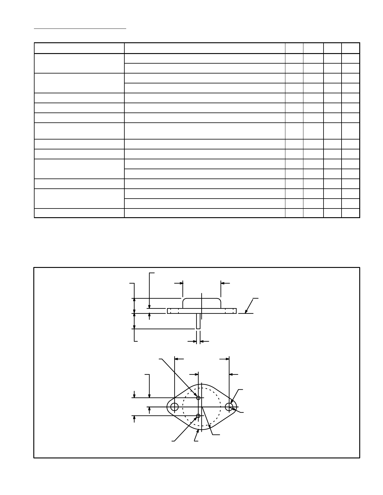
.350 (8.89)
.135 (3.45) Max
.875 (22.2)
Dia Max
Seating Plane
.312 (7.93) Min
.040 (1.02)
VIN
.215 (5.45)
.430
(10.92)
1.187 (30.16)
.665
(16.9)
.156 (3.96) Dia
(2 Holes)
.188 (4.8) R Max
Adjust
.525 (13.35) R Max
VOUT/Case
Share Link: