NLAS1053(2002) 데이터 시트보기 (PDF) - ON Semiconductor
부품명
상세내역
일치하는 목록
NLAS1053 Datasheet PDF : 12 Pages
| |||
NLAS1053
MAXIMUM RATINGS
Symbol
Parameter
Value
Unit
VCC
VIN
VIS
IIK
TSTG
TL
TJ
qJA
PD
MSL
Positive DC Supply Voltage
Digital Input Voltage (Select and Inhibit)
Analog Output Voltage (VCH or VCOM)
DC Current, Into or Out of Any Pin
Storage Temperature Range
Lead Temperature, 1 mm from Case for 10 Seconds
Junction Temperature under Bias
Thermal Resistance
Power Dissipation in Still Air at 85_C
Moisture Sensitivity
−0.5 to +7.0
−0.5 ≤ V is ≤ +7.0
−0.5 ≤ V is ≤ VCC +0.5
50
−65 to +150
260
+150
250
250
Level 1
V
V
V
mA
_C
_C
_C
_C/W
mW
FR
VESD
Flammability Rating
ESD Withstand Voltage
Oxygen Index: 30% – 35%
UL–94–VO (0.125 in)
Human Body Model (Note 2)
> 2000
V
Machine Model (Note 3)
200
Charged Device Model (Note 4)
N/A
ILatch–Up Latch–Up Performance
Above VCC and Below GND at 85_C (Note 5)
±300
mA
Maximum Ratings are those values beyond which damage to the device may occur. Exposure to these conditions or conditions beyond those
indicated may adversely affect device reliability. Functional operation under absolute–maximum–rated conditions is not implied. Functional
operation should be restricted to the Recommended Operating Conditions.
1. Measured with minimum pad spacing on an FR4 board, using 10 mm–by–1 inch, 2–ounce copper trace with no air flow.
2. Tested to EIA/JESD22–A114–A.
3. Tested to EIA/JESD22–A115–A.
4. Tested to JESD22–C101–A.
5. Tested to EIA/JESD78.
RECOMMENDED OPERATING CONDITIONS
Symbol
Characteristics
VCC
VIN
VIO
VIS
TA
tr, tf
Positive DC Supply Voltage
Digital Input Voltage (Select and Inhibit)
Static or Dynamic Voltage Across an Off Switch
Analog Input Voltage (CH, COM)
Operating Temperature Range, All Package Types
Input Rise or Fall Time,
(Enable Input)
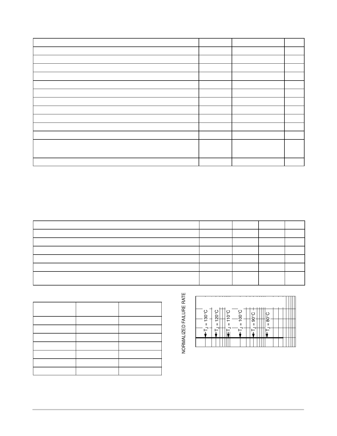
DEVICE JUNCTION TEMPERATURE VERSUS TIME
TO 0.1% BOND FAILURES
Junction
Temperature 5C
Time, Hours
Time, Years
80
1,032,200
117.8
90
419,300
47.9
100
178,700
20.4
110
79,600
9.4
120
37,000
4.2
130
17,800
2.0
140
8,900
1.0
Vcc = 3.3 V ± 0.3 V
Vcc = 5.0 V ± 0.5 V
Min
2.0
GND
GND
GND
−55
0
0
Max
5.5
5.5
VCC
VCC
+125
100
20
Unit
V
V
V
V
°C
ns/V
FAILURE RATE OF PLASTIC = CERAMIC
UNTIL INTERMETALLICS OCCUR
1
1
10
100
1000
TIME, YEARS
Figure 2. Failure Rate versus
Time Junction Temperature
http://onsemi.com
2
Share Link: 