NJU7044 데이터 시트보기 (PDF) - Japan Radio Corporation
부품명
상세내역
일치하는 목록
NJU7044
Japan Radio Corporation

NJU7044 Datasheet PDF : 5 Pages
| |||
Preliminary NJU7044
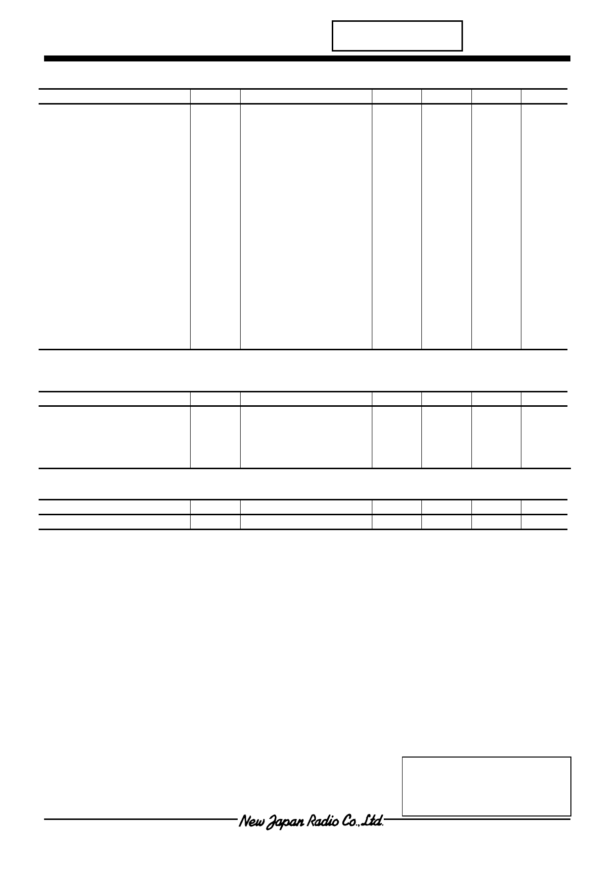
●DC CHARACTERISTICS
PARAMETER
Operating Current
Input Offset Voltage
Input Bias Current
Input Offset Current
Large Signal Voltage Gain
Common Mode Rejection Ratio
SYMBOL
IDD
VIO
IB
IIO
AV
CMR
TEST CONDITION
No Signal Apply
RL=10kΩ to 1.1V,
Vo=1.1V±1.0V
CMR+: 1.1V ≤ VCM ≤ 2.2V
CMR-: 0V ≤ VCM ≤ 1.1V
(Note 9)
MIN.
-
-
-
-
70
30
Supply Voltage Rejection Ratio
SVR
2.2V ≤ VDD ≤ 2.7V,
VCM=VDD/2
Output Voltage1
VOH1
RL=10kΩ to 1.1V
VOL1
RL=10kΩ to 1.1V
Output Voltage2
VOH2
RL=600Ω to 1.1V
VOL2
RL=600Ω to 1.1V
Output Source Current
Output Sink Current
ISOURCE
ISINK
VO=1.1V
VO=1.1V
Input Common Mode Voltage Range
VICM
CMR ≥ 30dB
(Note 9) CMR is represented by either CMR+ or CMR- has lower value.
45
2.15
-
2.1
-
10
10
0
●AC CHARACTERISTICS
PARAMETER
SYMBOL
TEST CONDITION
MIN.
Unity Gain Bandwidth
GB
RL=10kΩ to 1.1V
-
Total Harmonic Distortion
THD
f=1kHz, VIN=1Vpp, AV=0dB
-
Equivalent Input Noise Voltage
VNI
f=1kHz
-
Amp to Amp Separation
CS
f=1kHz, Vo=1.2Vpp
-
RL=2kΩ to 1.1V
●TRANSIENT CHARACTERISTICS
PARAMETER
SYMBOL
TEST CONDITION
MIN.
Slew Rate
SR
RL=10kΩ to 1.1V
-
(VDD=2.2V, Ta=25ûC)
TYP.
MAX.
UNIT
1.2
2
mA
-
10
mV
1
-
pA
1
-
pA
90
-
dB
60
-
dB
70
-
dB
-
-
V
-
0.05
V
-
-
V
-
0.1
V
15
-
mA
15
-
mA
-
2.2
V
TYP.
0.8
0.05
40
TBD
(VDD=2.2V, Ta=25ûC)
MAX.
UNIT
-
MHz
-
%
-
nV/√Hz
-
dB
(VDD=2.2V, Ta=25ûC)
TYP.
MAX.
UNIT
0.6
-
V/µs
Ver.2005-02-14
[CAUTION]
The specifications on this data book are only given for information,
without any guarantee as regards either mistakes or omissions. The
application circuits in this data book are described only to show
representative usages of the product and not intended for the
guarantee or permission of any right including the industrial rights.
-5-
Share Link: