NJU6533 데이터 시트보기 (PDF) - Japan Radio Corporation
부품명
상세내역
일치하는 목록
NJU6533 Datasheet PDF : 4 Pages
| |||
NJU6533
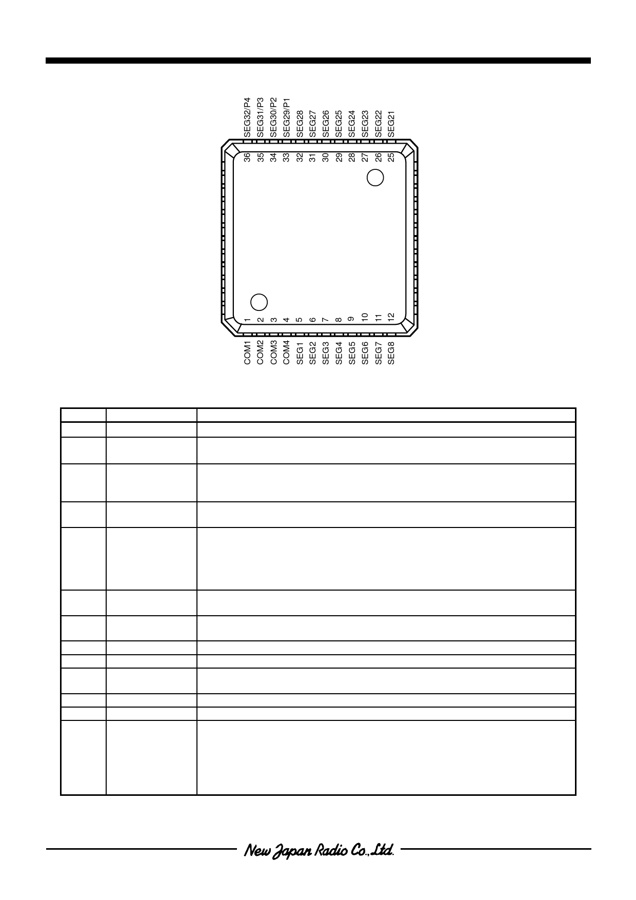
! PIN CONFIGURATION
VLCD
37
V1
38
V2
39
VSS
40
INHb
41
RSTb 42
CSb
43
SI
44
SCK
45
VDD
46
OSC1 47
OSC2 48
NJU6533
24 SEG20
23 SEG19
22 SEG18
21 SEG17
20 SEG16
19 SEG15
18 SEG14
17 SEG13
16 SEG12
15 SEG11
14 SEG10
13 SEG9
! TERMINAL DISCRIPTION
No.
46
37
38,
39
40
41
42
43
44
45
47,
48
1~4
5~32
33~36
Pad Name
VDD
VLCD
V1,
V2
VSS
INHb
RSTb
CSb
SI
SCK
OSC1,
OSC2
COM1 ~ COM4
SEG1 ~ SEG28
SEG29/P1 ~
SEG32 /P4
Function
Power supply: 3V /5V
LCD driving voltage
VLCD ≥ V1 ≥ V2 ≥ VSS, VLCD ≥VDD
Bias
At 1/3 bias ratio, keep V1- V2 open
At 1/2 bias ratio, short V1- V2
GND
VSS =0V
Display OFF
When INHb is "H", display is ON, and when INHb is "L", display is off.
When INHb is “L", all segment and common drivers output VSS, and the
oscillator stop operation. But, if at the same time RSTb="L", the oscillator
functions and all segment and common drivers output VSS
Reset
When RSTb is “L", command register and latch circuit is reset
Chip select
When CSb is "L", data can be read in.
Serial data input (8 bit=1word)
Serial clock
External resistor connection pin for CR oscillation, or external clock input pin.
When external clock is used, input the signal to OSC1 and keep OSC2 open.
Common driver outputs
Segment driver outputs
Segment driver outputs/general purpose output ports
These 4 pins can be used as segment driver outputs or general purpose output
ports by setting Command Register.
When selected as general purpose ports, data can be outputted via these ports
during COM1 timing.
According to transferred data, "H"=VDD or "L"=VSS will be outputted.
-2-
Ver.2004-03-05
Share Link: 