NJU6061 데이터 시트보기 (PDF) - Japan Radio Corporation
부품명
상세내역
일치하는 목록
NJU6061 Datasheet PDF : 2 Pages
| |||
NJU6061 Preliminary
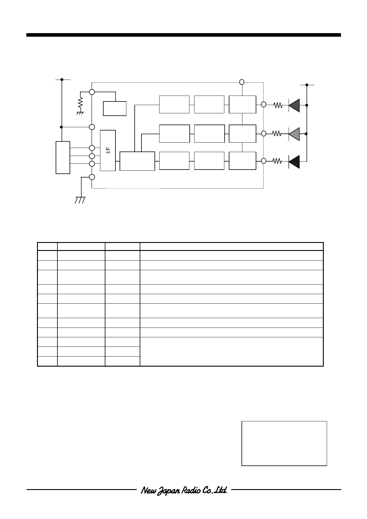
! BLOCK DIAGRAM
VDD
OSC
VDD
C CS
P CLK
U DATA
VSS
EN
OSC
Program
Register
128 step
PWM
Program
Register
128 step
PWM
Instruction
Decoder
Program
Register
128 step
PWM
Driver
30mA
Driver
30mA
Driver
30mA
LED1
LED2
LED3
VLED
! PIN DESCRIPTIONS
No. PIN NAME
VDD
RSTb
CSb
CLK
DATA
OSC
VSS
EN
LED1
LED2
LED3
TYPE
Power
Input
Input
Input
Input
Input
Power
Input
Output
Output
Output
DESCRIPTIONS
VDD Power Supply terminal
Reset terminal - Active “L”.
Chip Select terminal
The serial data is fixed on the rising edge of CSb clock.
Shift Clock terminal
Serial Data terminal
Oscillating terminal
External resistor connecting
Ground terminal
Output Enable terminal
LED Connect terminals (Open drain output)
Output level are 32 steps PWM by instruction control.
Connecting cathode of LED.
-2-
[CAUTION]
The specifications on this databook are only
given for information , without any guarantee
as regards either mistakes or omissions. The
application circuits in this databook are
described only to show representative usages
of the product and not intended for the
guarantee or permission of any right including
the industrial rights.
Ver.2004-03-09
Share Link: 