NCV8518B 데이터 시트보기 (PDF) - ON Semiconductor
부품명
상세내역
일치하는 목록
NCV8518B Datasheet PDF : 13 Pages
| |||
NCV8518B
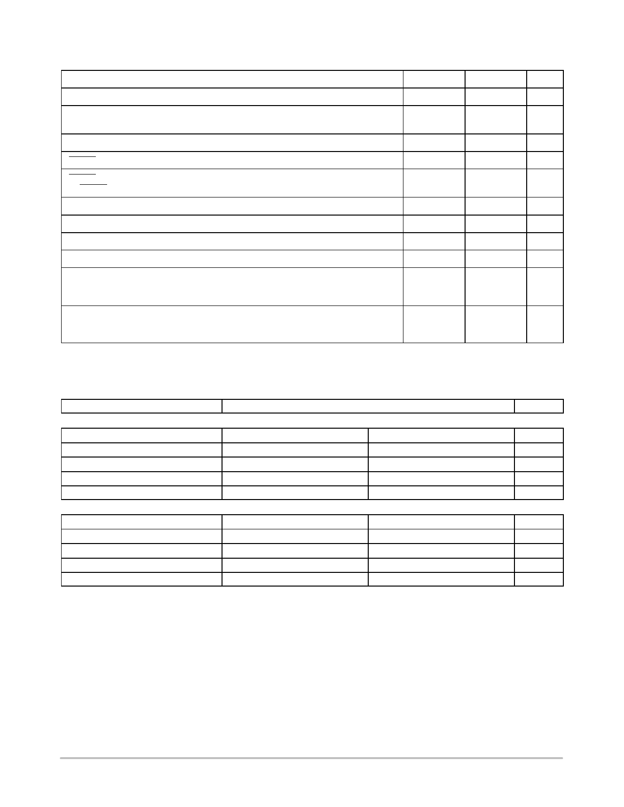
MAXIMUM RATINGS
Rating
Symbol
Value
Unit
Input Voltage
ENABLE Voltage
(ENABLE may be connected to VIN through an external 20k resistor without damage)
Output Voltage
RESET Voltage
RESET Current
(RESET may be incidentally shorted either to VOUT or to GND without damage)
ESD Susceptibility (Human Body Model)
VIN
VENABLE
VOUT
VRESET
IRESET
−
−0.3 to 45
V
−0.3 to 16
V
−0.3 to +7.0
V
0 V to VOUT
V
Internally
Limited
mA
2.0
kV
Logic Inputs/Outputs (Reset, WDI, Wake Up, Delay)
−
−0.3 to +7.0
V
Operating Junction Temperature
Storage Temperature Range
Moisture Sensitivity Level
SOIC−16 EP (Case 751R)
SOIC−8 EP (Case 751AC)
TJ
TS
MSL
−40 to150
°C
−55 to +150
°C
1
3
Lead Temperature Soldering: Reflow
Leaded Part
60−150 sec above 183°C, 30 sec max at peak
Lead−Free Part 60−150 sec above 217°C, 40 sec max at peak
−
240 peak
°C
−
265 peak
°C
Stresses exceeding Maximum Ratings may damage the device. Maximum Ratings are stress ratings only. Functional operation above the
Recommended Operating Conditions is not implied. Extended exposure to stresses above the Recommended Operating Conditions may affect
device reliability.
THERMAL CHARACTERISTICS
Parameter
Board/Mounting Conditions Typical Value
Unit
SO−8 Exposed Pad Package
100 sq. mm spreader board (Note 1) 1 sq. inch spreader board (Note 2)
Junction to case top (YJT)
14
Junction to lead1 (YJL1)
36
Junction to board (YJB) (Note 3)
15
Junction to ambient (qJA)
126
SO−16 Exposed Pad Package
14
°C/W
26
°C/W
14
°C/W
80
°C/W
100 sq. mm spreader board (Note 1) 1 sq. inch spreader board (Note 2)
Junction to case top (YJT)
20
20
°C/W
Junction to lead1 (YJL1)
41
26
°C/W
Junction to board (YJB) (Note 3)
12
12
°C/W
Junction to ambient (qJA)
113
70
°C/W
Specific notes on thermal characterization conditions:
All boards are 0.062” thick FR4, 3” square, with varying amounts of copper heat spreader, in still air (free convection) conditions. Numerical
values are derived from an axisymmetric finite−element model where active die area, total die area, flag area, pad area, and board area are
equated to the actual corresponding areas.
1. 1 oz copper, 100 mm2 (0.155 in2) spreader area (includes exposed pad).
2. 1 oz copper, 645 mm2 (1 in2) spreader area (includes exposed pad).
3. “board” is defined as center of exposed pad soldered to board; this is the recommended number to be used for thermal calculations, as it
best represents the primary heat flow path and is least sensitive to board and ambient properties.
http://onsemi.com
4
Share Link: 