NCP690(2009) 데이터 시트보기 (PDF) - ON Semiconductor
부품명
상세내역
일치하는 목록
NCP690
(Rev.:2009)
(Rev.:2009)
ON Semiconductor

NCP690 Datasheet PDF : 14 Pages
| |||
NCP690, NCP691, NCP692
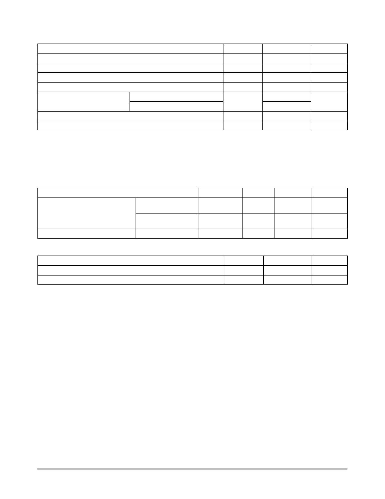
Table 3. ABSOLUTE MAXIMUM RATINGS
Rating
Symbol
Value
Unit
Input Voltage (Note 1)
Chip Enable Voltage
Output Voltage
Output Voltage / Sense Input, (SNS pin)
Electrostatic Discharge
Human Body Model
VIN
−0.3 to 6.5
V
VEN
−0.3 to 6.5
V
VOUT
−0.3 to 6.5
V
VSNS
−0.3 to 6.5
V
ESD
4000
V
Machine Model
400
Maximum Junction Temperature
TJ_MAX
150
_C
Storage Temperature Range
TSTG
−65 to 150
_C
Stresses exceeding Maximum Ratings may damage the device. Maximum Ratings are stress ratings only. Functional operation above the
Recommended Operating Conditions is not implied. Extended exposure to stresses above the Recommended Operating Conditions may affect
device reliability.
NOTE:
This device series contains ESD protection and exceeds the following tests:
ESD HBM tested per JEDEC standard: JESD22−A114
ESD MM tested per JEDEC standard: JESD22−A115
Latch–up Current Maximum Rating: ≤ 150 mA per JEDEC standard: JESD78
Table 4. PACKAGE THERMAL CHARACTERISTICS
Rating
Thermal Resistance,
Junction−to−Ambient (Note 2)
DFN6 3x3, 1 oz Cu
DFN6 3x3, 2 oz Cu
Thermal Resistance, Junction−to−Pin
Condition
64 mm2 Cu
645 mm2 Cu
64 mm2 Cu
645 mm2 Cu
Symbol
RqJA
RqJA
RqJL
Value
169
70
151
62
15
Unit
°C/W
°C/W
°C/W
Table 5. OPERATING RANGES
Rating
Symbol
Value
Unit
Operating Input Voltage (Notes 3 and 4)
VIN
1.5 to 6.0
V
Operating Junction Temperature Range
TJ
−40 to 125
°C
Operating Ambient Temperature Range
TA
−40 to 85
°C
1. Minimum VIN = (VOUT + VDO) or 1.5 V, whichever is higher.
2. Soldered on FR4 copper area, please refer to Applications Section for Safe Operating Area.
3. Minimum VIN = (VOUT + VDO) or 1.5 V, whichever is higher.
4. Refer to Electrical Characteristics and Application Information for Safe Operating Area.
http://onsemi.com
5
Share Link: