NCP690(2009) 데이터 시트보기 (PDF) - ON Semiconductor
부품명
상세내역
일치하는 목록
NCP690
(Rev.:2009)
(Rev.:2009)
ON Semiconductor

NCP690 Datasheet PDF : 14 Pages
| |||
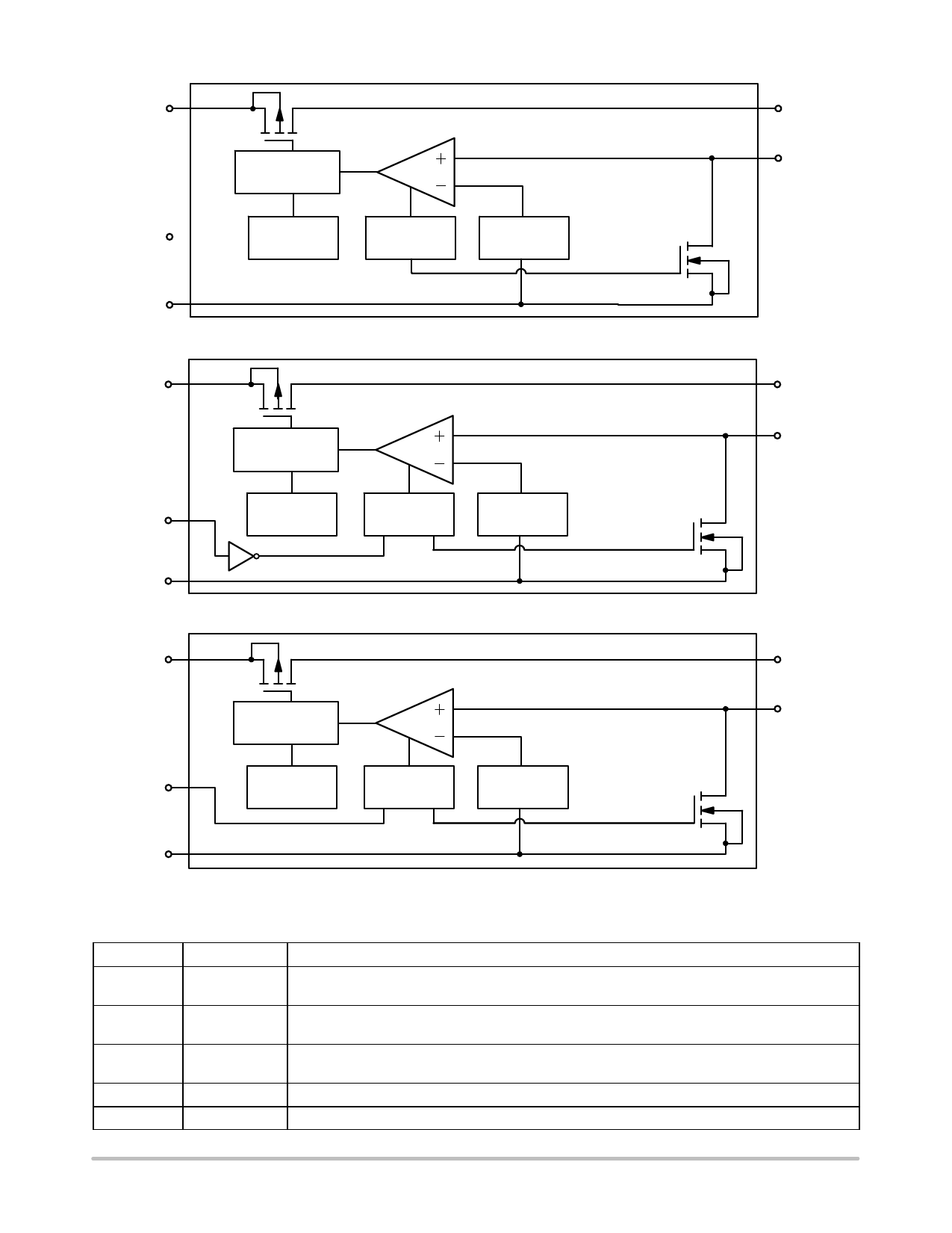
NCP690, NCP691, NCP692
IN
N/C
GND
MOSFET
DRIVER WITH
CURRENT LIMIT
THERMAL
SHUTDOWN
ENABLE
LOGIC
BANDGAP
REFERENCE
ACTIVE
DISCHARGE
Figure 8. NCP690 Block Diagram (Adjustable Version)
OUT
ADJ
IN
OUT
MOSFET
ADJ
DRIVER WITH
CURRENT LIMIT
EN
GND
THERMAL
SHUTDOWN
ENABLE
LOGIC
BANDGAP
REFERENCE
ACTIVE
DISCHARGE
Figure 9. NCP691 Block Diagram (Adjustable Version)
IN
OUT
MOSFET
ADJ
DRIVER WITH
CURRENT LIMIT
EN
THERMAL
SHUTDOWN
ENABLE
LOGIC
BANDGAP
REFERENCE
ACTIVE
DISCHARGE
GND
Figure 10. NCP692 Block Diagram (Adjustable Version)
Table 2. PIN FUNCTION DESCRIPTION FOR ADJUSTABLE VERSION
Pin No.
Pin Name
Description
1, 6
IN
Voltage inputs which supplies the current to the regulator. Both of these pins should be connected
together for full output current capability
2
GND
Power supply ground of the regulator. Connected to the die through the lead frame. Soldered to the
copper plane allows for effective heat removal.
3
EN
For NCP691 and NCP692 this pin functions as Enable Active Low and Enable Active High respect-
ively. For NCP690 this pin has no special meaning and should be left disconnected.
4
ADJ
Feedback input. Connect to middle point of resistor divider for Adjustable version.
5
OUT
Regulated output voltage
http://onsemi.com
4
Share Link: