NCP5173(2004) 데이터 시트보기 (PDF) - ON Semiconductor
부품명
상세내역
일치하는 목록
NCP5173 Datasheet PDF : 18 Pages
| |||
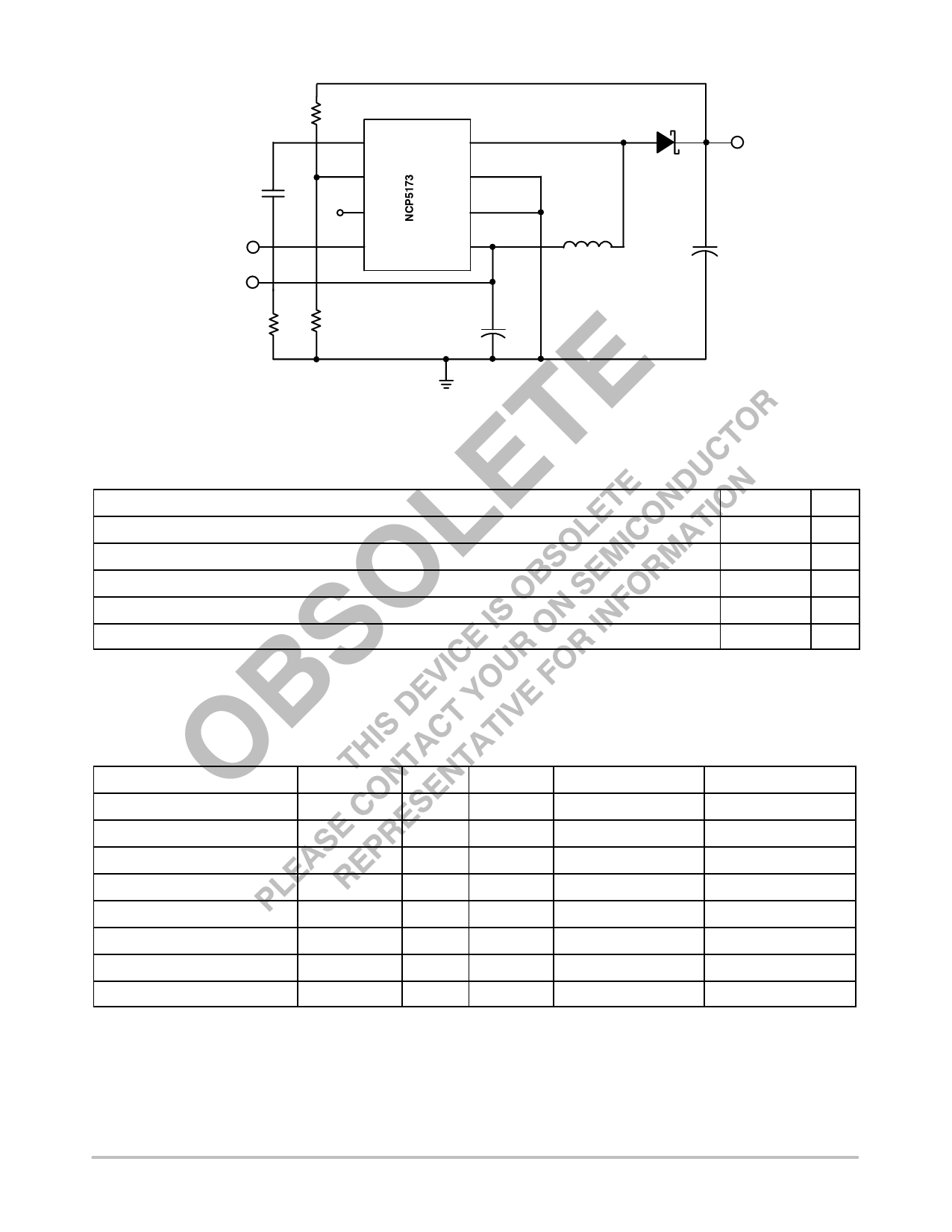
C1
0.01 mF
SS
3.3 V
R1
5k
NCP5173
R2
3.72 k
1
VC
2 FB
3
Test
4
SS
VSW 8
PGND 7
AGND 6
VCC 5
D1
MBRS120T3
VOUT
5V
L1
22 mH
+ C3
22 mF
R3
1.28 k
+
C2
22 mF
Figure 1. Applications Diagram
MAXIMUM RATINGS*
Rating
Value
Unit
Junction Temperature Range, TJ
Storage Temperature Range, TSTORAGE
Package Thermal Resistance: Junction−to−Ambient, RqJA
Lead Temperature Soldering: Reflow (Note 1)
−40 to +150
−65 to +150
35
230 Peak
°C
°C
°C/W
°C
ESD, Human Body Model
1.2
kV
Maximum ratings are those values beyond which device damage can occur. Maximum ratings applied to the device are individual stress limit
values (not normal operating conditions) and are not valid simultaneously. If these limits are exceeded, device functional operation is not implied,
damage may occur and reliability may be affected.
1. 60 second maximum above 183°C.
*The maximum package power dissipation must be observed.
MAXIMUM RATINGS
Pin Name
IC Power Input
Shutdown/Sync
Loop Compensation
Voltage Feedback Input
Test Pin
Power Ground
Analog Ground
Switch Input
Pin Symbol
VCC
SS
VC
FB
Test
PGND
AGND
VSW
VMAX
30 V
30 V
6.0 V
10 V
6.0 V
0.3 V
0V
40 V
VMIN
−0.3 V
−0.3 V
−0.3 V
−0.3 V
−0.3 V
−0.3 V
0V
−0.3 V
ISOURCE
N/A
1.0 mA
10 mA
1.0 mA
1.0 mA
4A
N/A
10 mA
ISINK
200 mA
1.0 mA
10 mA
1.0 mA
1.0 mA
10 mA
10 mA
3.0 A
http://onsemi.com
2
Share Link: 