NCV5104 데이터 시트보기 (PDF) - ON Semiconductor
부품명
상세내역
일치하는 목록
NCV5104 Datasheet PDF : 15 Pages
| |||
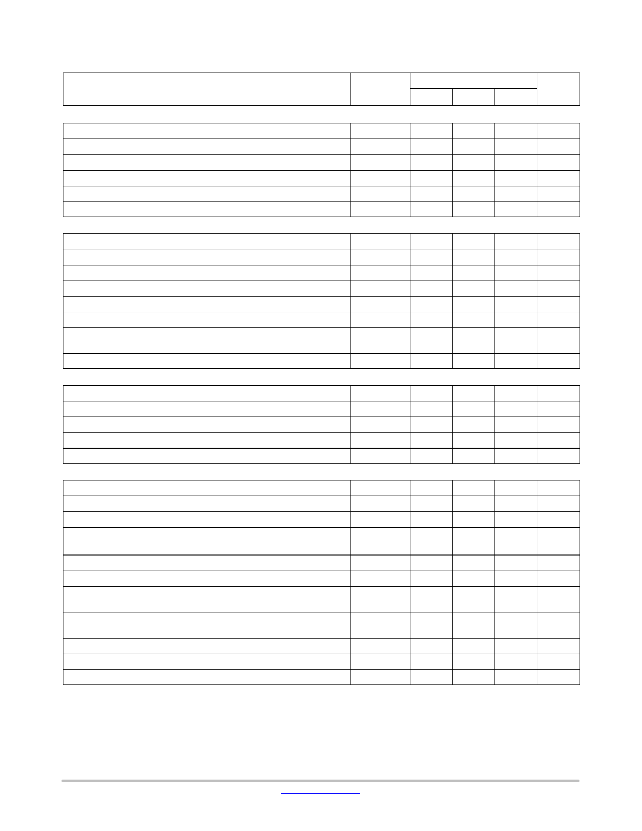
NCP5104, NCV5104
ELECTRICAL CHARACTERISTIC (VCC = Vboot = 15 V, VGND = Vbridge, −40°C < TJ < 125°C, Outputs loaded with 1 nF)
TJ −40°C to 125°C
Rating
Symbol
Min
Typ
Max
OUTPUT SECTION
Units
Output high short circuit pulsed current VDRV = 0 V, PW v 10 ms (Note 1)
IDRVsource
−
Output low short circuit pulsed current VDRV = Vcc, PW v 10 ms (Note 1)
IDRVsink
−
Output resistor (Typical value @ 25°C) Source
ROH
−
Output resistor (Typical value @ 25°C) Sink
ROL
−
High level output voltage, VBIAS−VDRV_XX @ IDRV_XX = 20 mA
VDRV_H
−
Low level output voltage VDRV_XX @ IDRV_XX = 20 mA
VDRV_L
−
DYNAMIC OUTPUT SECTION
250
−
mA
500
−
mA
30
60
W
10
20
W
0.7
1.6
V
0.2
0.6
V
Turn−on propagation delay (Vbridge = 0 V) (Note 2)
Turn−off propagation delay (Vbridge = 0 V or 50 V) (Note 3)
Shutdown propagation delay, when Shutdown is enabled
Shutdown propagation delay, when Shutdown is disabled
Output voltage rise time (from 10% to 90% @ VCC = 15 V) with 1 nF load
Output voltage fall time (from 90% to 10% @ VCC = 15 V) with 1 nF load
Propagation delay matching between the High side and the Low side
@ 25°C (Note 4)
tON
tOFF
tsd_en
tsd_dis
tr
tf
Dt
−
620
800
ns
−
100
170
ns
−
100
170
ns
−
620
800
ns
−
85
160
ns
−
35
75
ns
−
10
45
ns
Internal fixed dead time (Note 5)
DT
400
520
650
ns
INPUT SECTION
Low level input voltage threshold
Input pull−down resistor (VIN < 0.5 V)
High level input voltage threshold
Logic “1” input bias current @ VIN = 5 V @ 25°C
Logic “0” input bias current @ VIN = 0 V @ 25°C
SUPPLY SECTION
VIN
−
−
0.8
V
RIN
−
200
−
kW
VIN
2.3
−
−
V
IIN+
−
5
25
mA
IIN−
−
−
2.0
mA
Vcc UV Start−up voltage threshold
Vcc_stup
8.0
8.9
9.8
V
Vcc UV Shut−down voltage threshold
Vcc_shtdwn
7.3
8.2
9.0
V
Hysteresis on Vcc
Vcc_hyst
0.3
0.7
−
V
Vboot Start−up voltage threshold reference to bridge pin
(Vboot_stup = Vboot − Vbridge)
Vboot_stup
8.0
8.9
9.8
V
Vboot UV Shut−down voltage threshold
Vboot_shtdwn 7.3
8.2
9.0
V
Hysteresis on Vboot
Vboot_shtdwn 0.3
0.7
−
V
Leakage current on high voltage pins to GND
(VBOOT = VBRIDGE = DRV_HI = 600 V)
IHV_LEAK
−
5
40
mA
Consumption in active mode (Vcc = Vboot, fsw = 100 kHz and 1 nF load on
ICC1
−
4
5
mA
both driver outputs)
Consumption in inhibition mode (Vcc = Vboot)
ICC2
−
250
400
mA
Vcc current consumption in inhibition mode
ICC3
−
200
−
mA
Vboot current consumption in inhibition mode
ICC4
−
50
−
mA
Product parametric performance is indicated in the Electrical Characteristics for the listed test conditions, unless otherwise noted. Product
performance may not be indicated by the Electrical Characteristics if operated under different conditions.
1. Parameter guaranteed by design.
2. TON = TOFF + DT
3. Turn−off propagation delay @ Vbridge = 600 V is guaranteed by design.
4. See characterization curve for Dt parameters variation on the full range temperature.
5. Timing diagram definition see: Figure 4, Figure 5 and Figure 6.
www.onsemi.com
4
Share Link: 