NCP1251 데이터 시트보기 (PDF) - ON Semiconductor
부품명
상세내역
일치하는 목록
NCP1251 Datasheet PDF : 24 Pages
| |||
NCP1251
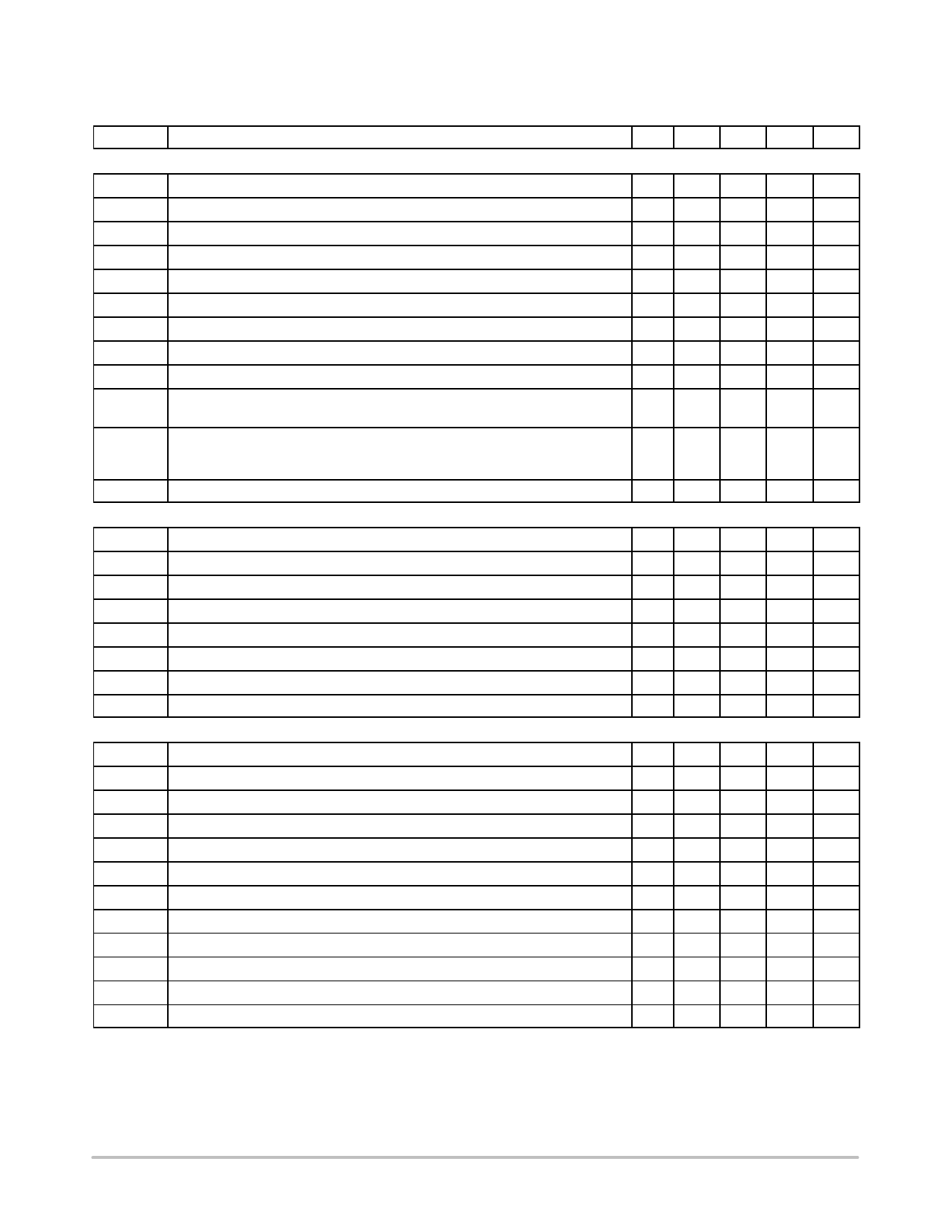
ELECTRICAL CHARACTERISTICS
(For typical values TJ = 25°C, for min/max values TJ = −40°C to +125°C, Max TJ = 150°C, VCC = 12 V unless otherwise noted)
Symbol
Rating
Pin Min Typ Max Unit
SUPPLY SECTION
VCCON
VCC(min)
VCCHYST
VZENER
ICC1
VCC increasing level at which driving pulses are authorized
VCC decreasing level at which driving pulses are stopped
Hysteresis VCCON − VCC(min)
Clamped VCC when latched off / burst mode activation @ ICC = 500 mA
Start−up current
5
16
18
20
V
5 8.2 8.8 9.4
V
5 6.0
V
5
7.0
V
5
15 mA
ICC2 Internal IC consumption with IFB = 50 mA, FSW = 65 kHz and CL = 0 nF
5
ICC3 Internal IC consumption with IFB = 50 mA, FSW = 65 kHz and CL = 1 nF
5
ICC2 Internal IC consumption with IFB = 50 mA, FSW = 100 kHz and CL = 0 nF
5
ICC3 Internal IC consumption with IFB = 50 mA, FSW = 100 kHz and CL = 1 nF
5
ICCstby Internal IC consumption while in skip cycle (VCC = 12 V, driving a typical 6 A/600 V 5
MOSFET)
1.4 2.2 mA
2.1 3.0 mA
1.7 2.5 mA
3.1 4.0 mA
550
mA
ICCLATCH Current flowing into VCC pin that keeps the controller latched (Note 4)
5
mA
TJ = −40°C to +125°C
40
TJ = 0°C to +125°C
32
Rlim
Current−limit resistor in series with the latch SCR
5
4.0
kW
DRIVE OUTPUT
Tr
Output voltage rise−time @ CL = 1 nF, 10−90% of output signal
Tf
Output voltage fall−time @ CL = 1 nF, 10−90% of output signal
ROH
Source resistance
ROL
Sink resistance
Isource Peak source current, VGS = 0 V – (Note 5)
Isink
Peak sink current, VGS = 12 V – (Note 5)
VDRVlow DRV pin level at VCC close to VCC(min) with a 33 kW resistor to GND
VDRVhigh DRV pin level at VCC = 28 V – DRV unloaded
CURRENT COMPARATOR
6
40
ns
6
30
ns
6
13
W
6
6.0
W
6
300
mA
6
500
mA
6 8.0
V
6
10
12
14
V
IIB
VLimit1
VLimit2
Vfold
Vfreeze
TDEL
TLEB
TSS
Input Bias Current @ 0.8 V input level on pin 4
Maximum internal current setpoint – TJ = 25°C – pin 3 grounded
Maximum internal current setpoint – TJ = −40°C to 125°C – pin 3 grounded
Default internal voltage set point for frequency foldback trip point – 45% of Vlimit
Internal peak current setpoint freeze ([31% of Vlimit)
Propagation delay from current detection to gate off−state
Leading Edge Blanking Duration
Internal soft−start duration activated upon startup, auto−recovery
4
0.02
mA
4 0.744 0.8 0.856 V
4 0.72 0.8 0.88 V
3
357
mV
3
250
mV
4
100 150 ns
4
300
ns
−
4
ms
IOPPo Setpoint decrease for pin 3 biased to –250 mV – (Note 6)
3
31.3
%
IOOPv
IOOPv
IOPPs
Voltage setpoint for pin 3 biased to −250 mV – (Note 6), TJ = 25°C
Voltage setpoint for pin 3 biased to −250 mV – (Note 6), TJ = −40°C to 125°C
Setpoint decrease for pin 3 grounded
3 0.51 0.55 0.60 V
3 0.50 0.55 0.62 V
3
0
%
4. For design robustness, we recommend to inject 60 mA as a minimum at the lowest input line voltage.
5. Guaranteed by design
6. See characterization table for linearity over negative bias voltage
7. A 1 MW resistor is connected from pin 3 to the ground for the measurement.
http://onsemi.com
5
Share Link: 