HI3197 데이터 시트보기 (PDF) - Intersil
부품명
상세내역
일치하는 목록
HI3197 Datasheet PDF : 25 Pages
| |||
HI3197
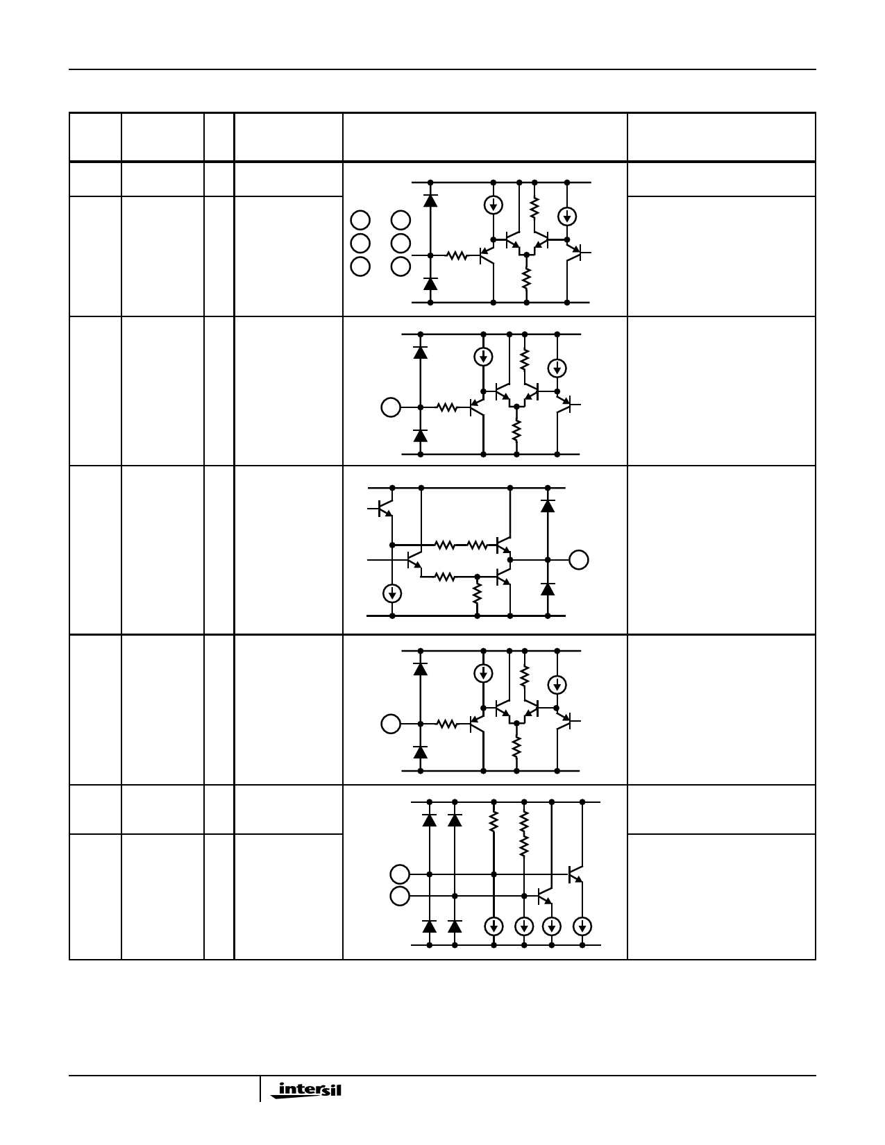
Pin Descriptions and I/O Pin Equivalent Circuits
PIN NO
1 to 6
45 to 48
7 to 16
SYMBOL
DA0 to DA9
DB0 to DA9
TYPICAL
VOLTAGE
I/O
LEVEL
I TTL
I TTL
EQUIVALENT CIRCUIT
DVCC1
1 TO 6
45 TO 48
7 TO 16
17
DIV2IN
I TTL
DGND1
DVCC1
DESCRIPTION
Side A Data Input.
Side B Data Input.
VREF
1/2 Frequency-Divided Clock Input.
Use this pin for MUX.1A or MUX.2
mode. Leave open for other modes.
17
VREF
18
DIV2OUT O TTL
DGND1
DVCC1
18
1p/u2t.FTrehqeuesnigcnya-Dl ivwidithedthCeloc1k/2
Out-
fre-
quency divided clock (DIV2OUT) is
output for MUX.1A mode. Leave
open for other modes.
19
CLK/T
I TTL
20
CLKP/E
I PECL
21
CLKN/E
I PECL
DVCC1
19
DGND1
DVCC1
20
21
DGND1
DGND1
Clock Input. Use this pin when the
clock is input in the TTL level. At
this time, leave Pins 20 and 21
open.
VREF
Clock Input. Use this pin when the
clock is input in PECL level. At this
time, leave Pin 19 open.
CLKP/E Complementary Input.
When left open, this pin goes to
the threshold potential. Operation
is possible only with CLKP/E, but
complementary input is recom-
mended to attain fast and stable
operation.
3
Share Link: 