NB2309AI1HDG(2015) 데이터 시트보기 (PDF) - ON Semiconductor
부품명
상세내역
일치하는 목록
NB2309AI1HDG Datasheet PDF : 9 Pages
| |||
NB2309A
Zero Delay and Skew Control
All outputs should be uniformly loaded to achieve Zero
Delay between input and output. Since the CLKOUT pin is
the internal feedback to the PLL, its relative loading can
adjust the input−output delay.
For applications requiring zero input−output delay, all
outputs, including CLKOUT, must be equally loaded. Even
if CLKOUT is not used, it must have a capacitive load equal
to that on other outputs, for obtaining zero−input−output
delay.
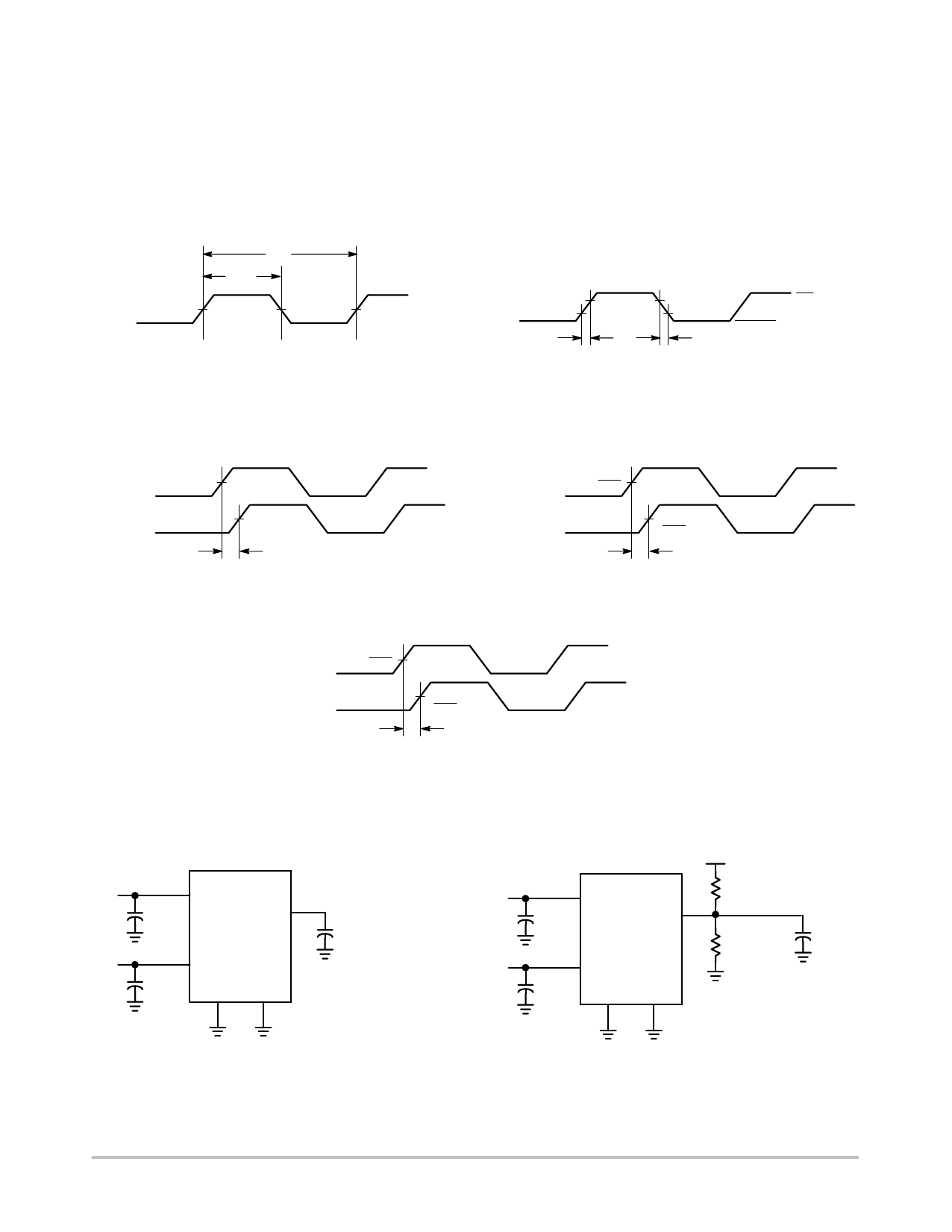
SWITCHING WAVEFORMS
1.4 V
t1
t2
1.4 V
1.4 V
Figure 3. Duty Cycle Timing
OUTPUT
2.0 V
0.8 V
t3
2.0 V
0.8 V
t4
3.3 V
0V
Figure 4. All Outputs Rise/Fall Time
OUTPUT
1.4 V
OUTPUT
t5
1.4 V
Figure 5. Output − Output Skew
VDD
2
INPUT
VDD
OUTPUT
2
t6
Figure 6. Input − Output Propagation Delay
CLKOUT, Device 1
CLKOUT, Device 2
VDD
2
VDD
2
t7
Figure 7. Device − Device Skew
VDD
CLKOUT
0.1 mF
OUTPUTS
CLOAD
VDD
0.1 mF GND GND
TEST CIRCUITS
VDD
0.1 mF
OUTPUTS
VDD
0.1 mF GND GND
VDD
1 kW
1 kW
10 pF
Figure 8. Test Circuit #1
Figure 9. Test Circuit #2
For parameter t8 (output slew rate) on −1H devices
www.onsemi.com
6
Share Link: 