NB2309AI1DTG(2015) 데이터 시트보기 (PDF) - ON Semiconductor
부품명
상세내역
일치하는 목록
NB2309AI1DTG Datasheet PDF : 9 Pages
| |||
NB2309A
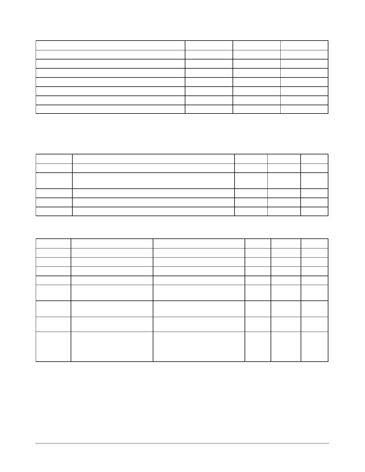
Table 3. MAXIMUM RATINGS
Parameter
Min
Max
Unit
Supply Voltage to Ground Potential
−0.5
+7.0
V
DC Input Voltage (Except REF)
DC Input Voltage (REF)
−0.5
VDD + 0.5
V
−0.5
7
V
Storage Temperature
−65
+150
°C
Maximum Soldering Temperature (10 sec)
260
°C
Junction Temperature
150
°C
Static Discharge Voltage (per MIL−STD−883, Method 3015)
>2000
V
Stresses exceeding those listed in the Maximum Ratings table may damage the device. If any of these limits are exceeded, device functionality
should not be assumed, damage may occur and reliability may be affected.
Table 4. RECOMMENDED OPERATING CONDITIONS
Parameter
Description
Min
Max
Unit
VDD
Supply Voltage
TA
Operating Temperature (Ambient Temperature)
3.0
Industrial
−40
Commercial
0
3.6
V
85
°C
70
CL
Load Capacitance, below 100 MHz
30
pF
CL
Load Capacitance, from 100 MHz to 133 MHz
10
pF
CIN
Input Capacitance
7
pF
Functional operation above the stresses listed in the Recommended Operating Ranges is not implied. Extended exposure to stresses beyond
the Recommended Operating Ranges limits may affect device reliability.
Table 5. ELECTRICAL CHARACTERISTICS VCC = 3.0 V to 3.6 V, GND = 0 V, TA = −40°C to +85°C
Parameter
Description
Test Conditions
Min
Max
Unit
VIL
Input LOW Voltage (Note 5)
0.8
V
VIH
Input HIGH Voltage (Note 5)
2.0
V
IIL
Input LOW Current
VIN = 0 V
50.0
mA
IIH
Input HIGH Current
VIN = VDD
100.0
mA
VOL
Output LOW Voltage
IOL = 8 mA (−1)
IOL = 12 mA (−1H)
0.4
V
VOH
Output HIGH Voltage
IOH = −8 mA (−1)
IOH = −12 mA (−1H)
2.4
V
IDD
Supply Current (Commercial Temp) Unloaded outputs at 66.67 MHz,
Select inputs at VDD
34
mA
IDD
Supply Current (Industrial Temp)
Unloaded outputs at 100 MHz
66.67 MHz
33 MHz
Select inputs at VDD or GND, at Room
Temp
50
mA
34
19
Product parametric performance is indicated in the Electrical Characteristics for the listed test conditions, unless otherwise noted. Product
performance may not be indicated by the Electrical Characteristics if operated under different conditions.
5. REF input has a threshold voltage of VDD/2.
www.onsemi.com
4
Share Link: 