CY7C4201-10(2002) 데이터 시트보기 (PDF) - Cypress Semiconductor
부품명
상세내역
일치하는 목록
CY7C4201-10 Datasheet PDF : 18 Pages
| |||
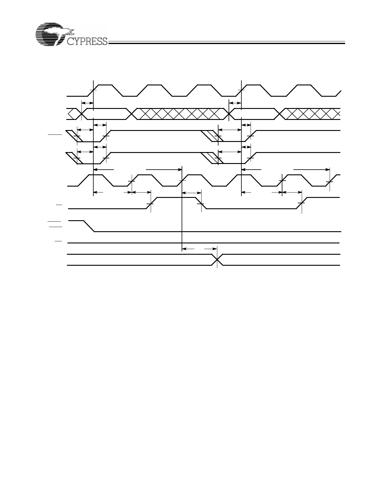
Switching Waveforms (continued)
Read Cycle Timing
RCLK
REN1,REN2
tENS
EF
tCLKH
tCKL
tCLKL
tENH
tREF
tA
NO OPERATION
Q0 –Q8
OE
WCLK
tOLZ
tOE
[15]
tSKEW1
WEN1
CY7C4421/4201/4211/4221
CY7C4231/4241/4251
tREF
VALID DATA
tOHZ
WEN2
Reset Timing[16]
RS
REN1,
REN2
tRS
tRSS
tRSS
tRSR
tRSR
WEN1
WEN2/LD [17]
tRSS
tRSR
EF,PAE
tRSF
tRSF
FF,PAF,
Q0 - Q8
tRSF
OE=1 [18]
OE=0
Notes:
14. tSKEW1 is the minimum time between a rising RCLK edge and a rising WCLK edge to guarantee that FF will go HIGH during the current clock cycle. If the time
between the rising edge of RCLK and the rising edge of WCLK is less than tSKEW1, then FF may not change state until the next WCLK rising edge.
15. tSKEW1 is the minimum time between a rising WCLK edge and a rising RCLK edge to guarantee that EF will go HIGH during the current clock cycle. It the time
between the rising edge of WCLK and the rising edge of RCLK is less than tSKEW1, then EF may not change state until the next RCLK rising edge.
Document #: 38-06016 Rev. *A
Page 9 of 18
Share Link: 