MT9041 데이터 시트보기 (PDF) - Mitel Networks
부품명
상세내역
일치하는 목록
MT9041 Datasheet PDF : 14 Pages
| |||
MT9041
Advance Information
Functional Description
The MT9041 is a fully digital, phase-locked loop
designed to provide timing references to interface
circuits for T1 and E1 Primary Rate Digital
Transmission links. As shown in Figure 1, the PLL
employs a high resolution Digitally Controlled
Oscillator (DCO) to generate the T1 and E1 outputs.
The interface circuit on the output of the DCO
generates 1.544 MHz (C1.5), 3.088 MHz (C3), 2.048
MHz (C2), 4.096 MHz (C4), 8.192 MHz (C8), 16.384
MHz (C16), and three 8 kHz frame pulses F0o, FP8-
STB, and FP8-GCI.
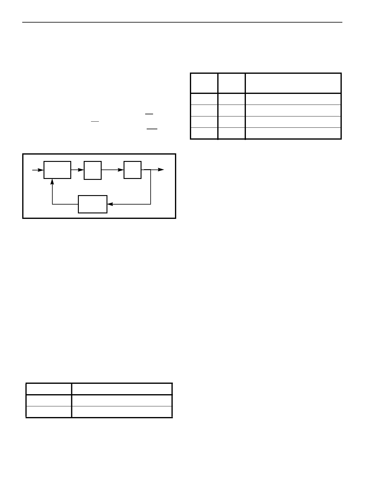
Phase
fref Detector
Loop
Filter
DCO
fsync
Divider
Figure 3 - PLL Block Diagram
As shown in Figure 3, the PLL of the MT9041
consists of a phase detector (PD), a loop filter, a high
resolution DCO, and a digital frequency divider. The
digitally controlled oscillator (DCO) is locked in
frequency (n x fref) to one of three possible reference
frequencies, configured using pins FSEL1 and
FSEL2. The PLL is capable of providing a full range
of E1/T1 clock signals synchronized to the primary
PRI input. The loop filter is a first order lowpass
structure that provides approximately a 2 Hz
bandwidth.
Modes of Operation
The MT9041 can operate in one of two modes,
NORMAL or FREERUN, as controlled by mode
select pin MS (see Table 1).
MS
Description of Operation
0
NORMAL
1
FREERUN
Table 1- Operating Modes of the MT9041
Normal Mode
.
There are three possible input frequencies for
selection as the primary reference clock. These are 8
kHz, 1.544 MHz or 2.048 MHz. Frequency selection
3-86
is controlled by the logic levels of FSEL1 and FSEL2,
as shown in Table 2. This variety of input frequencies
was chosen to allow the generation of all the
necessary T1 and E1 clocks from either a T1, E1 or
frame pulse reference source.
FSEL FSEL
2
1
Input Reference
Frequency
0
0
0
1
Reserved
8 kHz
1
0
1
1
1.544 MHz
2.048 MHz
Table 2 - Input Frequency Selection of the MT9041
PLL Measures of Performance
To meet the requirements of AT & T TR62411 and
ETSI 300 011, the following PLL performance
parameters were measured:
• locking range and lock time
• free-run accuracy
• intrinsic jitter
• jitter transfer function
• output jitter spectrum
• wander
Locking Range and Lock Time
The locking range of the PLL is the range that the
input reference frequency can be deviated from its
nominal frequency while the output signals maintain
synchronization. The relevant value is usually
specified in parts-per-million (ppm). For both the T1
and E1 outputs, lock was maintained while an 8 kHz
input was varied between 7900 Hz to 8100 Hz
(corresponding to ±12500 ppm). This is well beyond
the required ±100 ppm. The lock range of 12500
ppm also applies to 1.544 MHz and 2.048 MHz
reference inputs.
The lock time is a measure of how long it takes the
PLL to reach steady state frequency after a
frequency step on the reference input signal. The
locking time is measured by applying an 8000 Hz
signal to the primary reference and an 8000.8 Hz
(+100 ppm) to the secondary reference. The output
is monitored with a time interval analyzer during slow
periodic rearrangements on the reference inputs.
The lock time for both the T1 and E1 outputs is
approximately 311 ms, which is well below the
required lock time of 1.0 seconds.
Share Link: 