PI74FCT2861TQ 데이터 시트보기 (PDF) - Pericom Semiconductor
부품명
상세내역
일치하는 목록
PI74FCT2861TQ Datasheet PDF : 4 Pages
| |||
PI74FCT2861T 1122334455667788990011223344556677889900112233445566778899001122112233445566778899001122334455667788990011223344556677889900112211223344556677889900112233445566778899001122334455667788990011221122334455667788990011223344556677889900112233445566778899001122112233445566778899001122
10-Bit Non-Inverting BusTransceiver
Product Features
PI74FCT2861T is pin compatible with bipolar FAST
Series at a higher speed and lower power consumption
25Ω series resistor on all outputs
TTL input and output levels
Extremely low static power
Hysteresis on all inputs
Industrial operating temperature range: 40°C to +85°C
Packages available:
24-pin 300 mil wide plastic DIP (P24)
24-pin 150 mil wide plastic QSOP (Q24)
24-pin 150 mil wide plastic TQSOP (R24)
24-pin 300 mil wide plastic SOIC (S24)
Product Description
Pericom Semiconductors PI74FCT series of logic circuits are
produced in the Companys advanced 0.8 micron CMOS technology,
achieving industry leading speed grades.
The PI74FCT286T bus transceiver provides high-performance bus
interface buffering for wide data/address paths carrying parity.
They are designed for high-capacitance load drive capability while
providing bus loading at both inputs and outputs.
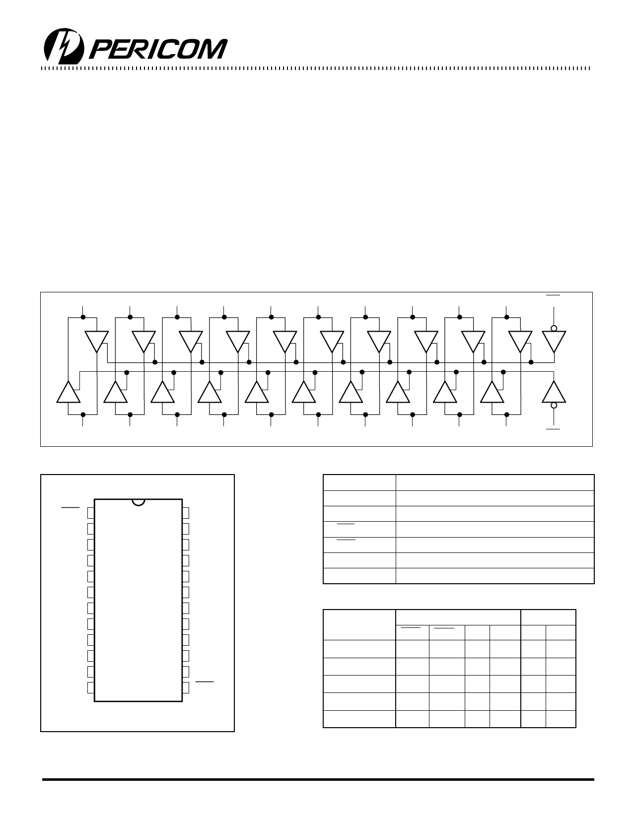
Logic Block Diagram
T0
T1
T2
T3
T4
T5
T6
T7
T8
T9
OER
R0
R1
R2
R3
R4
R5
R6
R7
R8
R9
OET
10-Bit Product Configuration
OER 1
24 Vcc
R0 2
23 T0
R1 3
22 T1
R2 4
R3 5
R4 6
R5 7
24-PIN 21 T2
P24
20 T3
Q24
R24
19 T4
S24 18 T5
R6 8
17 T6
R7 9
16 T7
R8 10
15 T8
R9 11
14 T9
GND 12
13 OET
Product Pin Description
Pin Name
RN
TN
OERN
OETN
GND
VCC
Description
Receive Inputs/Outputs
Transmit Inputs/Outputs
Output Enable Receive Mode
Output Enable Transmit Mode
Ground
Power
Truth Table(1) (Non-inverting)
Function
High-Z
Inputs
OETN OERN RN TN
H H XX
Transmitting L H L N/A
Transmitting L H H N/A
Receiving
H L N/A L
Receiving
H L N/A H
Outputs
RN TN
ZZ
N/A L
N/A H
L N/A
H N/A
Note:
1. H = High Voltage Level L = Low Voltage Level
X = Don't Care
NA = Not Applicable
Z = High Impedance
1
PS8339 09/29/98
Share Link: 