NJU6676CH 데이터 시트보기 (PDF) - Japan Radio Corporation
부품명
상세내역
일치하는 목록
NJU6676CH
Japan Radio Corporation

NJU6676CH Datasheet PDF : 46 Pages
| |||
NJU6676
PRELIMINARY
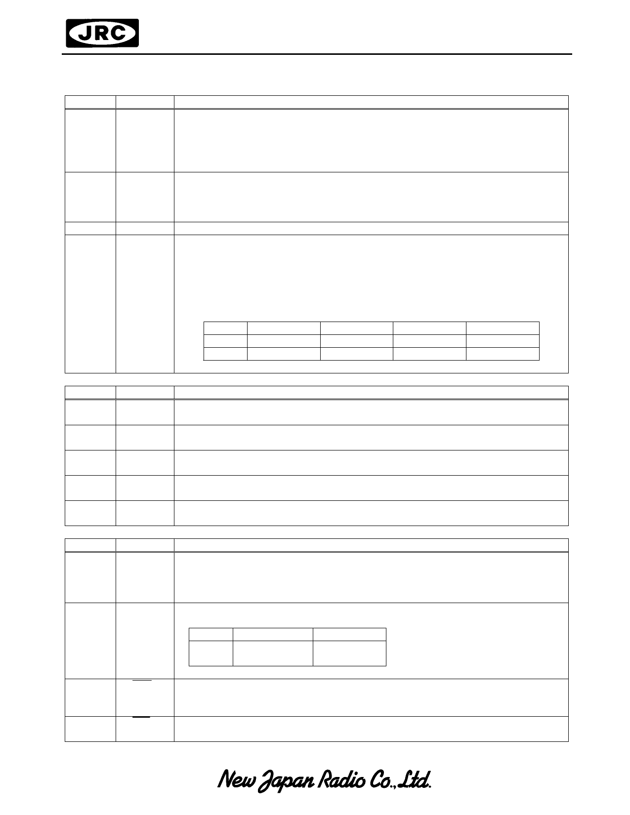
■ TERMINAL DESCRIPTION
Power Supply Peripheral
No. Symbol
Description
11,17
26∼29
51,52
65∼67
73,75
VDD VDD=+3V
8,14,
VSS VSS=0V
3031,
32,49
50,70,74
33∼36 VSS2 Reference voltage for voltage booster
53,54
55,56
57,58
59,60
61,62
V1 LCD Driving Voltage Supplying Terminal. When the internal voltage booster
V2 is not used, supply each level of LCD driving voltage from outside with
V3 following relation.
V4 VDD≥V1≥V2≥V3≥V4≥V5
V5
When the internal power supply is on, the internal circuits generate and
supply following LCD bias voltage from V1 to V4 terminal.
Bias
V1
V2
V3
V4
1/7 Bias V5+6/7VLCD V5+5/7VLCD V5+2/7VLCD V5+1/7VLCD
1/9 Bias V5+8/9VLCD V5+7/9VLCD V5+2/9VLCD V5+1/9VLCD
(VLCD=VDD-V5)
LCD Driving Power Supply Peripheral
No. Symbol
Description
41,42
C1+ Boosted capacitor connecting terminals used for voltage booster.
43,44
C1-
47,48
C2+ Boosted capacitor connecting terminals used for voltage booster.
45,46
C2-
39,40
C3- Boosted capacitor connecting terminals used for voltage booster.
37,38
Vout Voltage booster output terminal. Connect the boosted capacitor between
this terminal and VSS2.
63,64
VR Voltage adjust terminal. V5 level is adjusted by external bleeder resistance
connecting between VDD and V5 terminal.
MPU Interface Peripheral
No. Symbol
Description
18∼25 D0∼D7 P/S="H" : Tri-state bi-directional Data I/O terminal in 8-bit parallel operation.
(24,25) (SCL, P/S="L" : D7=Serial data input terminal. D6=Serial data clock signal input
SI)
terminal. Data from SI is loaded at the rising edge of SCL and
latched as the parallel data at 8th rising edge of SCL.
13
A0 Connect to the Address bus of MPU. The data on the D0 to D7 is
distinguished between Display data and Instruction by status of A0.
A0
H
L
Distin
.
Display Data
Instruction
12
RES Reset terminal. When the RES terminal goes to “L”, the initialization is
performed.
Reset operation is executing during “L” state of RES.
9
CS1 Chip select terminal. Data Input/Output are available during CS1=”L” and
10
CS2 CS2=”H”.
Share Link: