MP3276 데이터 시트보기 (PDF) - Exar Corporation
부품명
상세내역
일치하는 목록
MP3276 Datasheet PDF : 16 Pages
| |||
MP3276
Fault Protected 16 Channel, 12-Bit
Data Acquisition Subsystem
FEATURES
• Fault Protected 16-Channel 12-Bit A/D
Converter with Sample & Hold, Reference,
Clock and 3-state Outputs
• Fast Conversion, less than 15µS
• Microprocessor Bus Interface
• 2’s Complement Data Output
• Parallel or Serial Data Output Modes
• 65 ns Bus Access Time
• Remote Analog Ground Sensing
• Overvoltage Protected Input (50 V over the Sup-
ply Voltages)
• Precision Reference for Long Term Stability and
Low Gain T.C.
• Guaranteed Linearity Over Temperature
• Guaranteed Performance at +12/–5 V, ±12 & ±15 V
• Low Power: 110 mW typ. (7 mW per Channel typ.)
• 32 Channel Version: MP3274
GENERAL DESCRIPTION
The MP3276 is a complete 16-channel, 12-bit Data Acquisi-
tion Subsystem with 3-state output buffers for direct interfacing
to 16-bit microprocessor buses. Implemented using an ad-
vanced BiCMOS process, the converter combines a 16-channel
passive overvoltage protected multiplexer instrumentation amp,
a sample & hold, a SAR, a 12-bit decoded D/A, a comparator, a
precision reference and the control logic to achieve an accurate
repeated conversion in less than 15µs, and a mux/instrumenta-
tion amp settling period of less than 10µs.
A unique input design provides input overvoltage protection
to 50 V over the supply voltages. The circuit design can allow
for an overvoltage condition on unselected channels without dis-
rupting the measured channel or operation of the MP3276! The
internal 4 V reference has sufficient output current to provide
other system reference needs. Precision thin film scaling and
offset resistors are laser trimmed to provide for less than 2 LSB
INL for +10 V inputs on all channels.
In addition, the MP3276 will output either full scale (0111 ....)
for overrange and – full scale (1000....) for underrange condi-
tions. This greatly simplifies microprocessor software develop-
ment.
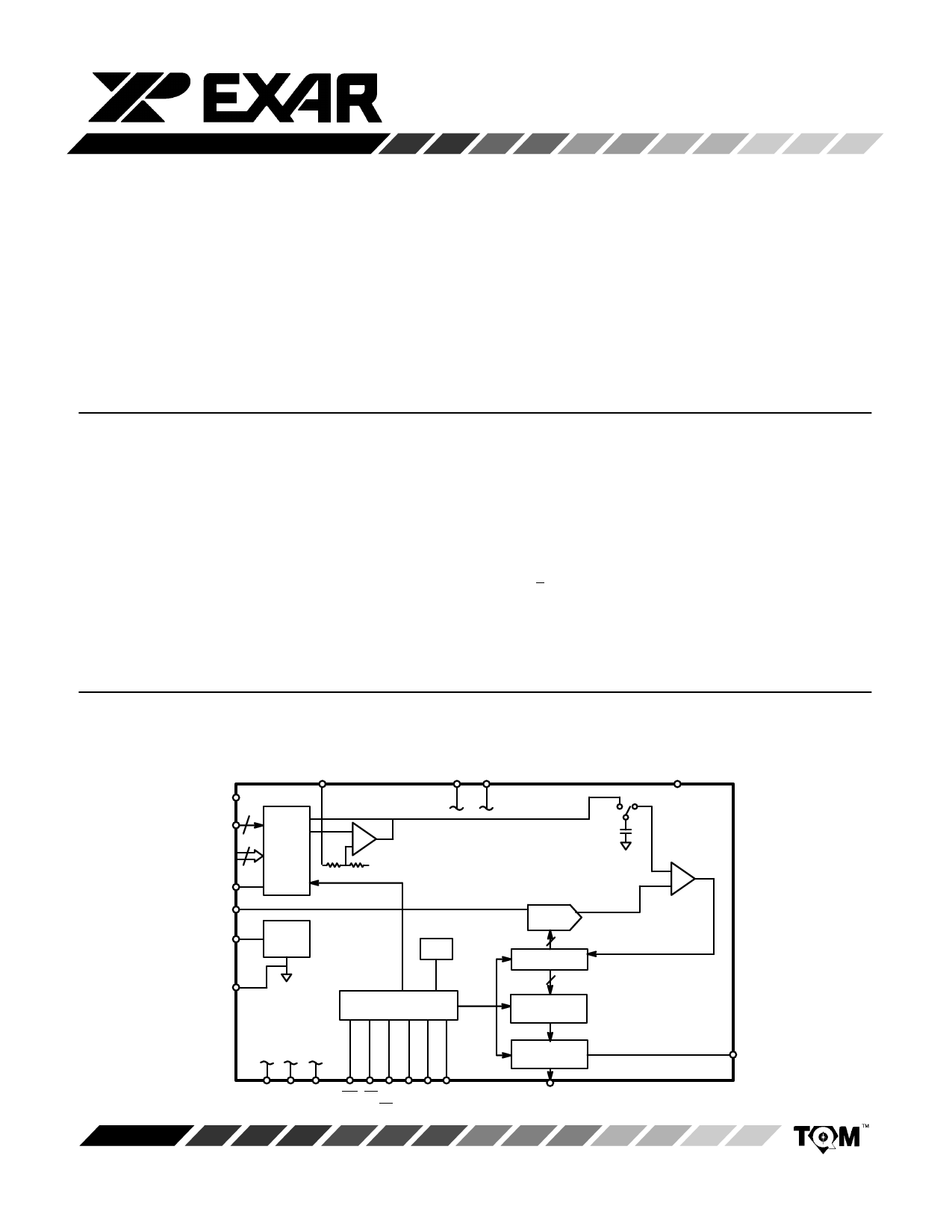
SIMPLIFIED BLOCK DIAGRAM
GND
GND REF.
VDD VCC
AB0-3
(4 pins) 4 16 Ch.
AIN0-15
MUX
(16 pins)
16
AGND2
REF IN
–
+
REF IN /2
VREF
4V
REF OUT
REF
CLK
AGND3
Control
Logic
VDAC
12
SAR
12
Latch/
Shift Register
3-state
Drivers
Rev. 4.00
DGND VEE AGND WR RD ADEN STL
CS
STS
1
DB0-DB11
AGND
Comp
PXS
Share Link: 