MP3275 데이터 시트보기 (PDF) - Exar Corporation
부품명
상세내역
일치하는 목록
MP3275 Datasheet PDF : 16 Pages
| |||
MP3275
APPLICATION INFORMATION
The MP3275 is a complete A/D converter system, with its
own built-in reference and clock. It may be used by itself (“stand-
alone” operation), or it may be interfaced with a microprocessor.
Successful application of the MP3275 requires careful atten-
tion to four main areas:
1) Physical layout.
2) Connection/Trimming according to mode of operation.
3) Conditioning of input signals.
4) Control and Timing considerations.
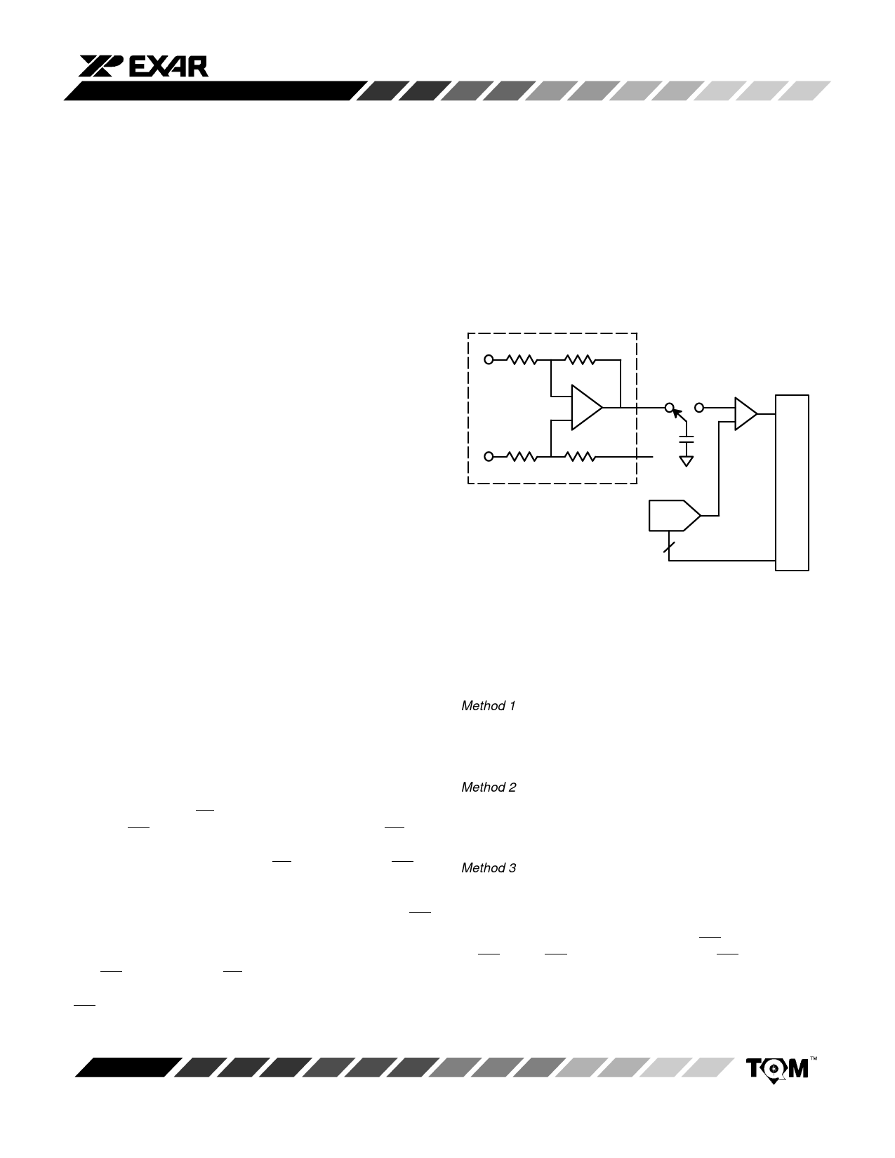
Ground Reference
The ground reference pin can be used for remote ground
sensing of a common mode input signal with a maximum 6 V p-p
around AGND.
This common input can also be used to dither each input’s
“zero”. By averaging multiple conversions digitally, higher reso-
lution for each input conversion can be obtained. Patterns for
this dither can be a ramp, a stair step, or white noise.
Physical Layout
The 12-bit accuracy of the MP3275 represents a dynamic
range of 72dB. Precautions must be taken to avoid any interfer-
ing signals, whether conducted or radiated, to assure that this is
not degraded.
130k
26k
1 of 16
COMP
• Avoid placing the chip and its analog signals near logic
traces. In general, using a double sided printed circuit
GND Ref.
card with a good ground plane on the component side is
recommended. Routing analog signals between ground
130k
26k
1/2
VREF
S
A
traces will help isolate digital control logic. If these lines
R
cross, do so at right angles. The GND Ref. is the positive
VDAC
terminal of the MUX/Instrumentation amplifier and will
provide common mode noise rejection. It should be
12
close to and shielded together with the channel inputs in
order to take advantage of this feature.
• Power supplies should be quiet and well regulated.
Grounds should be tied together at the package and
back to the system ground with a single path. Bypass the
supplies at the device with a 0.01 to 0.1µF ceramic cap
and a 10-47 µF tantalum type, in parallel.
Figure 7. Equivalent Input Circuit
Quasi Differential Sampling
“Stand-Alone” Operation
The MP3275 can be used in “stand-alone” operation, which is
useful in systems not requiring full computer bus interface capa-
bility.
For this operation, CS = 0, ADEN = 1, and conversion is con-
trolled by WR. The 3-state buffer SDO is enabled when RD goes
low. There are two possible conditions that the 3-state buffer
could be in during a conversion. If RD goes low prior to WR the
output buffer is enabled and the data from the previous conver-
sion is available at the outputs during STL = 1. At the end of the
present conversion which is initiated at the rising edge of WR,
STS returns low and the new conversion result is placed on the
output data buffer.
If WR goes low prior to RD, the data buffer remains in a high
impedance state and conversion is initiated at the rising edge of
WR. Upon the end of the conversion the STS returns low and
the conversion result is placed on the output data buffers.
Rev. 4.00
Method 1
For remote ground sensing where the remote ground does
not change more than 3 V from the A/D ground, connect GND
Ref to the remote ground.
Method 2
Where Method 1 applies to each channel or group of chan-
nels, add a mux to allow connecting the appropriate ground to
GND Ref.
Method 3
Use two parts. Tie both GND Ref pins together and connect
this node to the “common” remote GND. Control the sample
point by connecting each STL through an “OR” gate whose out-
put is “NAND” connect with WR (inverted WR). Use this output
as WR to both WR inputs. By controlling the WR, sample delay
differences between the two converters is minimized. Two parts
from the same date code will further minimize this difference.
Treat one A/D as the (+) terminal and the other as the (–) termi-
nal of the differential signal. Now the difference can be taken
digitally.
11
Share Link: 