FSTU6800 데이터 시트보기 (PDF) - Fairchild Semiconductor
부품명
상세내역
일치하는 목록
FSTU6800
Fairchild Semiconductor

FSTU6800 Datasheet PDF : 5 Pages
| |||
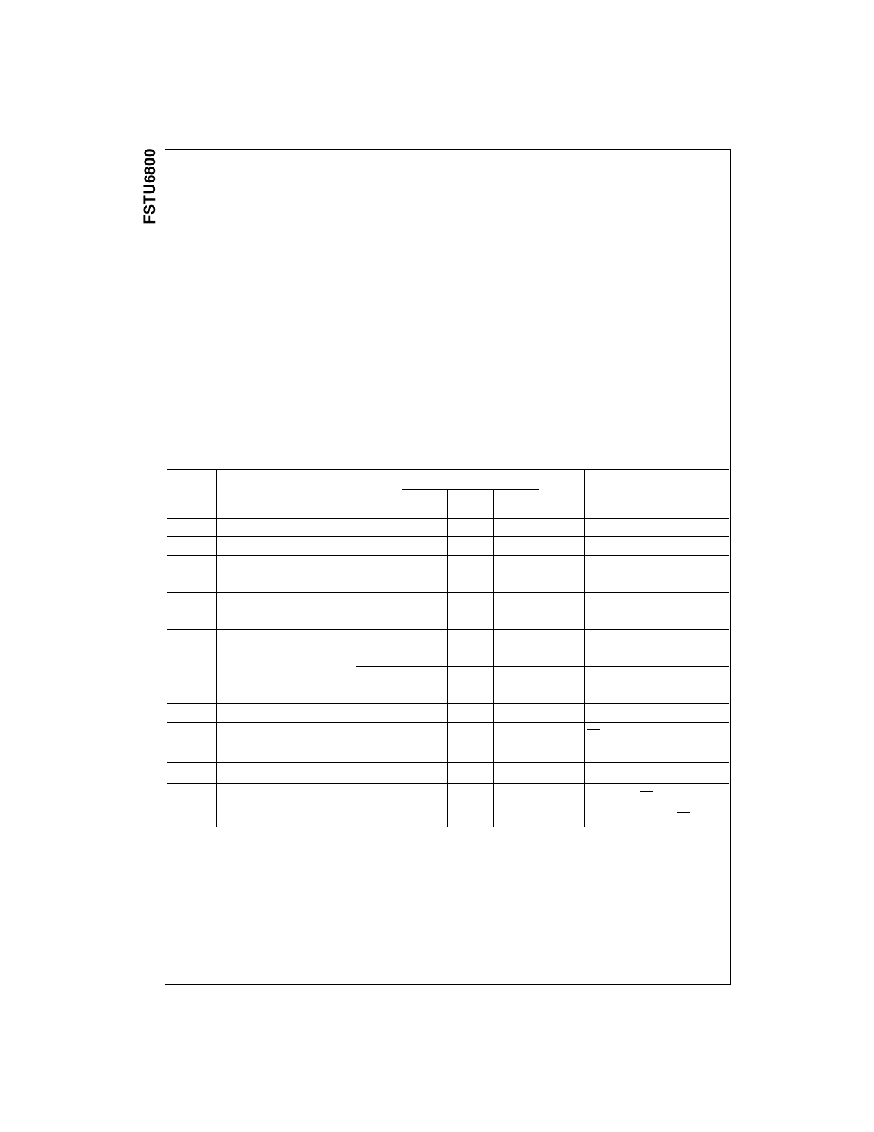
Absolute Maximum Ratings(Note 1)
Supply Voltage (VCC)
DC Switch Voltage (VS)
Bias V Voltage Range
DC Input Voltage (VIN) (Note 2)
DC Input Diode Current (lIK) VIN< 0V
DC Output (IOUT) Sink Current
DC VCC/GND Current (ICC/IGND)
Storage Temperature Range (TSTG)
−0.5V to +7.0V
−2.0V to +7.0V
−0.5V to +7.0V
−0.5V to +7.0V
−50mA
128mA
+/− 100mA
−65°C to +150 °C
DC Electrical Characteristics
Recommended Operating
Conditions (Note 3)
Power Supply Operating (VCC)
Precharge Supply (BiasV)
Input Voltage (VIN)
Output Voltage (VOUT)
Input Rise and Fall Time (tr, tf)
Switch Control Input
4.0V to 5.5V
1.5V to VCC
0V to 5.5V
0V to 5.5V
0 nS/V to 5 nS/V
Switch I/O
0nS/V to DC
Free Air Operating Temperature (TA) −40 °C to +85 °C
Note 1: The Absolute Maximum Ratings are those values beyond which
the safety of the device cannot be guaranteed. The device should not be
operated at these limits. The parametric values defined in the Electrical
Characteristics tables are not guaranteed at the absolute maximum ratings.
The Recommended Operating Conditions tables will define the conditions
for actual device operation.
Note 2: The input and output negative voltage ratings may be exceeded if
the input and output diode current ratings are observed.
Note 3: Unused control inputs must be held HIGH or LOW. They may not
float.
Symbol
Parameter
TA = −40 °C to +85 °C
VCC
(V)
Min
Typ
Max
Units
(Note 5)
Conditions
VIK
Clamp Diode Voltage
4.5
−1.2
V
IIN = −18mA
VIH
HIGH Level Input Voltage
4.0–5.5
2.0
V
VIL
LOW Level Input Voltage
4.0–5.5
0.8
V
II
Input Leakage Current
5.5
±1.0
µA 0 ≤ VIN ≤ 5.5V
IO
Output Current
4.5
0.25
mA BiasV = 2.4V, B = 0
IOZ
OFF-STATE Leakage Current
5.5
±1.0
µA
0 ≤ A ≤ VCC, VIN = VIH
RON
Switch On Resistance
4.5
4
7
Ω
VS = 0V, IIN = 64 mA
(Note 4)
4.5
4
7
Ω
VS = 0V, IIN = 30 mA
4.5
8
15
Ω
VS = 2.4V, IIN = 15 mA
4.0
11
20
Ω
VS = 2.4V, IIN = 15 mA
ICC
Quiescent Supply Current
5.5
3
µA
VS = VCC or GND, IOUT = 0
∆ ICC
Increase in ICC per Input
5.5
2.5
mA OE input at 3.4V
Other inputs at VCC or GND
IBIAS
Bias Pin Leakage Current
5.5
±1.0
µA OE = 0V, B = 0V, BiasV = 5.5V
IOZU
Switch Undershoot Current
5.5
100
µA
IIN = −20 mA, OE = 5.5V, VOUT ≥ VIH
VIKU
Voltage Undershoot
5.5
−2.0
V
0.0 mA ≥ IIN ≥ −50 mA, OE = 5.5V
Note 4: Measured by the voltage drop between A and B pins at the indicated current through the switch. On resistance is determined by the lower of the
voltages on the two (A or B) pins.
Note 5: Typical values are at VCC = 5.0V and TA= +25°C
www.fairchildsemi.com
2
Share Link: