MM74HC595 데이터 시트보기 (PDF) - Fairchild Semiconductor
부품명
상세내역
일치하는 목록
MM74HC595 Datasheet PDF : 14 Pages
| |||
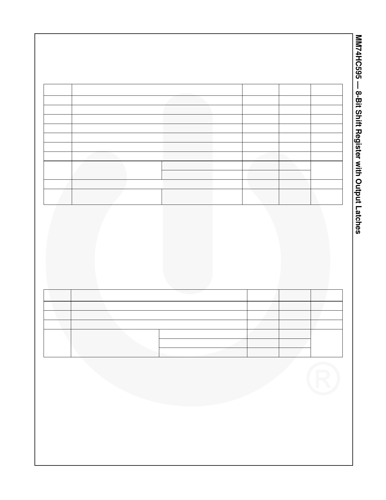
Absolute Maximum Ratings(1)
Stresses exceeding the absolute maximum ratings may damage the device. The device may not function or be
operable above the recommended operating conditions and stressing the parts to these levels is not recommended.
In addition, extended exposure to stresses above the recommended operating conditions may affect device
reliability. The absolute maximum ratings are stress ratings only.
Symbol
Parameter
Min.
Max.
VCC
VIN
VOUT
IIK, IOK
IOUT
ICC
TSTG
PD
Supply Voltage
DC Input Voltage
DC Output Voltage
Clamp Diode Current
DC Output Current, per Pin
DC VCC or GND Current, per Pin
Storage Temperature Range
Power Dissipation
PDIP(2)
SOIC Package Only
-0.5
-1.5 to VCC+
-0.5 to VCC+
-65
7.0
1.5
0.5
±20
±35
±70
+150
600
500
TL
ESD
Lead Temperature
Electrostatic Discharge Capability
Human Body Model,
JESD22-A114
+260
4000
Notes:
1. Unless otherwise specified all voltages are referenced to ground.
2. Power dissipation temperature derating, plastic package (PDIP);12mW/°C from -65 to +85°C.
Unit
V
V
V
mA
mA
mA
°C
mW
°C
V
Recommended Operating Conditions
The Recommended Operating Conditions table defines the conditions for actual device operation. Recommended
operating conditions are specified to ensure optimal performance to the datasheet specifications. Fairchild does not
recommend exceeding them or designing to Absolute Maximum Ratings.
Symbol
Parameter
VCC Supply Voltage
VIN, VOUT DC Input or Output Voltage
TA Operating Temperature Range
tR,tF Input Rise and Fall Times
VCC=2.0V
VCC=4.5V
VCC=6.0V
Min.
2
0
-40
Max.
6
VCC
+85
1000
500
400
Unit
V
V
°C
ns
© 1983 Fairchild Semiconductor Corporation
MM74HC595 • Rev. 1.0.2
4
www.fairchildsemi.com
Share Link: 