MM74HC373 데이터 시트보기 (PDF) - Fairchild Semiconductor
부품명
상세내역
일치하는 목록
MM74HC373 Datasheet PDF : 8 Pages
| |||
September 1983
Revised May 2005
MM74HC373
3-STATE Octal D-Type Latch
General Description
The MM74HC373 high speed octal D-type latches utilize
advanced silicon-gate CMOS technology. They possess
the high noise immunity and low power consumption of
standard CMOS integrated circuits, as well as the ability to
drive 15 LS-TTL loads. Due to the large output drive capa-
bility and the 3-STATE feature, these devices are ideally
suited for interfacing with bus lines in a bus organized sys-
tem.
When the LATCH ENABLE input is HIGH, the Q outputs
will follow the D inputs. When the LATCH ENABLE goes
LOW, data at the D inputs will be retained at the outputs
until LATCH ENABLE returns HIGH again. When a high
logic level is applied to the OUTPUT CONTROL input, all
outputs go to a high impedance state, regardless of what
signals are present at the other inputs and the state of the
storage elements.
The 74HC logic family is speed, function, and pin-out com-
patible with the standard 74LS logic family. All inputs are
protected from damage due to static discharge by internal
diode clamps to VCC and ground.
Features
s Typical propagation delay: 18 ns
s Wide operating voltage range: 2 to 6 volts
s Low input current: 1 PA maximum
s Low quiescent current: 80 PA maximum (74 Series)
s Output drive capability: 15 LS-TTL loads
Ordering Code:
Order Number Package Number
Package Description
MM74HC373WM
M20B
20-Lead Small Outline Integrated Circuit (SOIC), JEDEC MS-013, 0.300" Wide
MM74HC373SJ
M20D
20-Lead Small Outline Package (SOP), EIAJ TYPE II, 5.3mm Wide
MM74HC373MTC
MTC20
20-Lead Thin Shrink Small Outline Package (TSSOP), JEDEC MO-153, 4.4mm Wide
MM74HC373N
N20A
20-Lead Plastic Dual-In-Line Package (PDIP), JEDEC MS-001, 0.300" Wide
Devices also available in Tape and Reel. Specify by appending the suffix letter “X” to the ordering code.
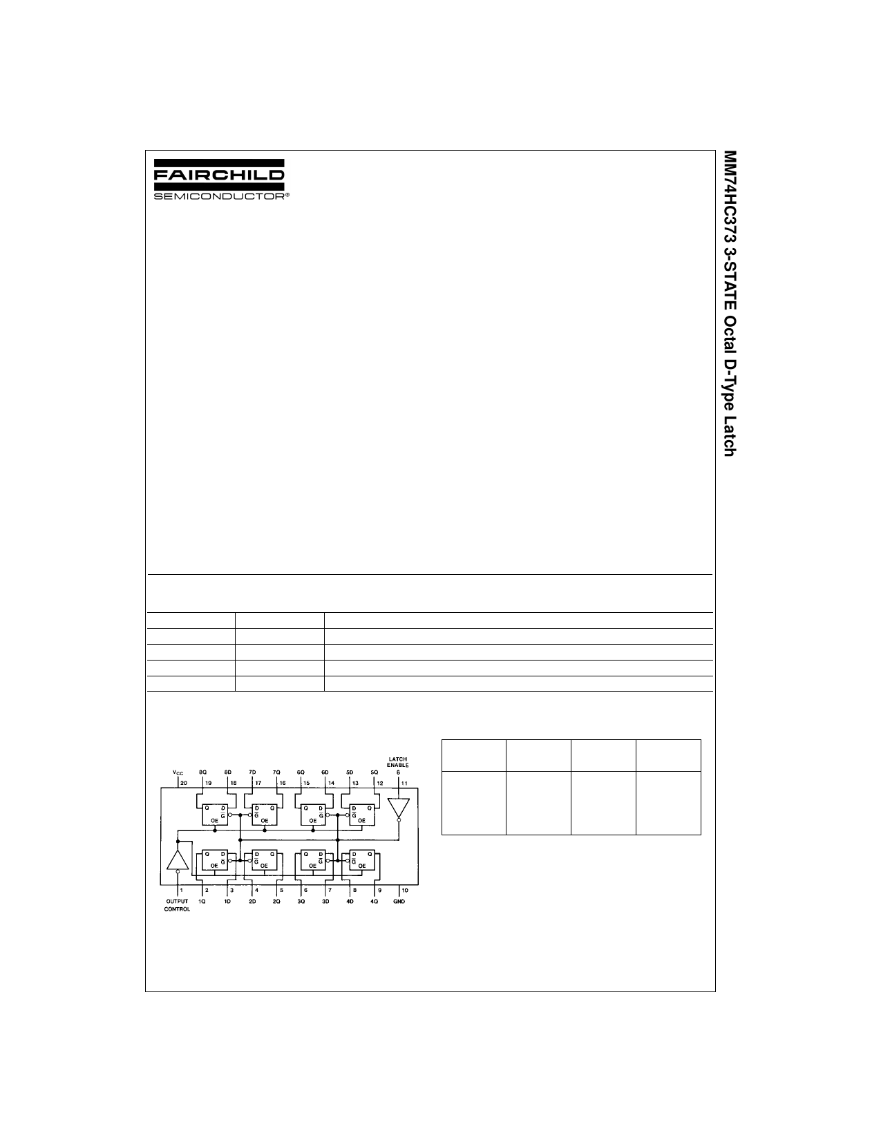
Connection Diagram
Truth Table
Pin Assignments for DIP, SOIC, SOP and TSSOP
Output
Latch
Data
373
Control
Enable
Output
L
H
H
H
L
H
L
L
L
L
X
Q0
H
X
X
Z
H HIGH Level
L LOW Level
Q0 Level of output before steady-state input conditions were established.
Z High Impedance
Top View
© 2005 Fairchild Semiconductor Corporation DS005335
www.fairchildsemi.com
Share Link: 