MK50H28 데이터 시트보기 (PDF) - STMicroelectronics
부품명
상세내역
일치하는 목록
MK50H28 Datasheet PDF : 64 Pages
| |||
MK50H28
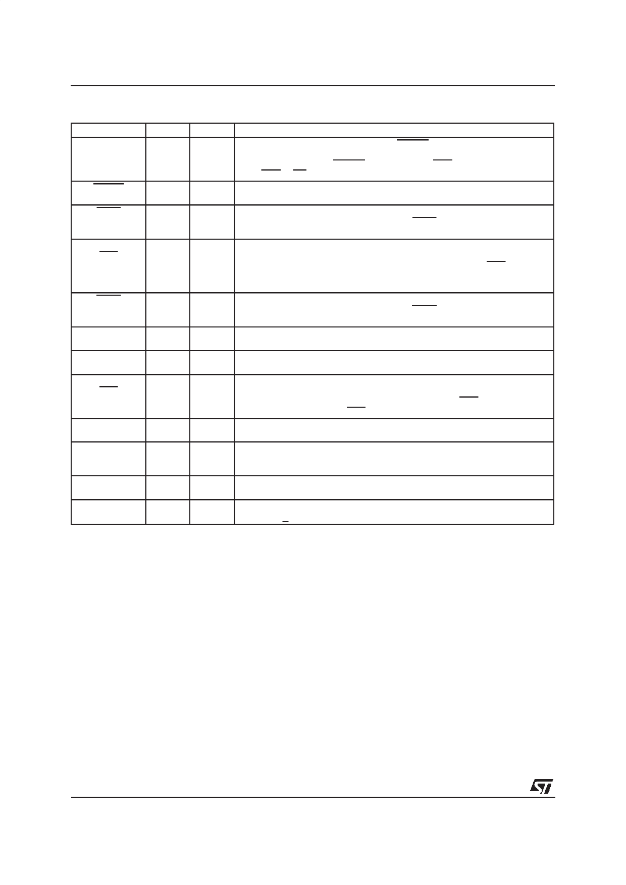
Table 1: PIN DESCRIPTION (continued)
SIGNAL NAME PIN(S)
RESET
23
[25]
TCLK
25
[28]
DTR
26
RTS
[29]
RCLK
27
[30]
SYSCLK
28
[31]
TD
29
[32]
DSR
30
CTS
[33]
RD
A<23:16>
VSS-GND
VCC
31
[34]
32-39
[37-43]
1,24
[1,26]
48
[52]
TYPE
I
I
IO
I
I
O
IO
I
o/3s
DESCRIPTION
As a Bus Slave, the MK50H28 asserts READY when it has put data on the
DAL lines during a READ cycle or is about to take data from the DAL lines
during a WRITE cycle. READY is a response to DAS and it will be released
after DAS or CS is negated.
RESET is the Bus signal that will cause MK50H28 to cease operation, clear
its internal logic and enter an idle state with the Power Off bit of CSR0 set.
TRANSMIT CLOCK. A 1x clock input for transmitter timing. TD changes on
the falling edge of TCLK. The frequency of TCLK may not be greater than
the frequency of SYSCL
DATA TERMINAL READY, REQUEST TO SEND. Modem control pin. Pin
26 is configurable through CSR5. This pin can be programmed to behave as
output RTS or as programmable IO pin DTR. If configured as RTS, the
MK50H28 will assert this pin if it has data to send and throughout the
transmission of a signal unit.
RECEIVE CLOCK. A 1x clock input for receiver timing. RD is sampled on
the rising edge of RCLK. The frequency of RCLK may not be greater than
the frequency of SYSCLK.
SYSTEM CLOCK. System clock used for internal timing of the MK50H28.
SYSCLK should be as defined in the Electrical Specifications in Section 5.
TRANSMIT DATA. Transmit serial data output.
DATA SET READY, CLEAR TO SEND. Modem Control Pin. Pin 30 is
configurable through CSR5. This pin can be programmed to behave as input
CTS or as programmable IO pin DSR. If configured as CTS, the MK50H28
will transmit all ones while CTS is high.
RECEIVE DATA. Received serial data input.
Address bits <23:16> used in conjunction with DAL<15:00> to produce a 24
bit address. MK50H28 drives these lines only as a Bus Master. A23-A20
may be driven continuously as described in the CSR4<7> BAE bit.
Ground Pins
Power Supply Pin
+5.0 VDC + 5%
SECTION 3
OPERATIONAL DESCRIPTION
The STMicroelectronics MK50H28 Multi-Logical
Link Communications Controller device is a VLSI
product intended for high performance data com-
munication applications requiring Frame Relay
Service on Permanent Virtual Circuits. The
MK50H28 will perform all frame formatting, such
as: frame delimiting with flags, FCS (CRC) gen-
eration and detection, and zero bit insertion and
deletion for transparency. The MK50H28 also in-
cludes a buffer management mechanism that al-
lows the user to transmit and/or receive multiple
frames for each active channel or DLCI. Con-
tained in the buffer management is an on-chip
dual channel DMA: one channel for receive and
one channel for transmit.
The MK50H28 can be used with any popular 16
6/64
or 8 bit microprocessor. A possible system con-
figuration for the MK50H28 is shown in Figure 1.
This document assumes that the processor has a
byte addressable memory organization.
The MK50H28 will move multiple blocks of re-
ceive and transmit data directly in and out of
memory through the Host’s bus.
The MK50H28 may be operated in full or half du-
plex mode. In half duplex mode the RTS and
CTS modem control pins are provided. In full du-
plex mode, these pins become user programma-
ble I/O pins.
All signal pins on the MK50H28 are TTL compat-
ible. This has the advantage of making the
MK50H28 independent of the physical interface.
As shown in Fig. 1, line drivers and receivers are
used for electrical connection to the physical
layer.
Share Link: 