MC74VHC4066 데이터 시트보기 (PDF) - ON Semiconductor
부품명
상세내역
일치하는 목록
MC74VHC4066 Datasheet PDF : 14 Pages
| |||
MC74VHC4066
VIS
0.1 μF
fin
VCC
VOS
TO
ON
DISTORTION
RL
CL*
METER
VCC/2
SELECTED VCC
7 CONTROL
INPUT
*Includes all probe and jig capacitance.
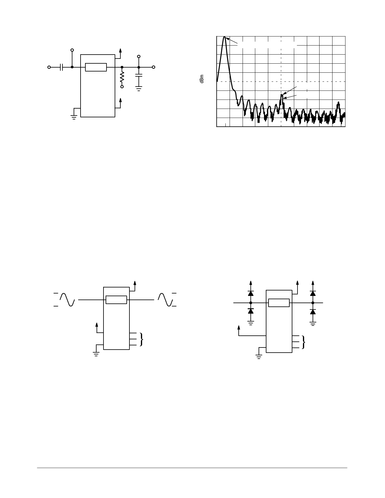
Figure 20. Total Harmonic Distortion, Test Set−Up
0
- 10
FUNDAMENTAL FREQUENCY
- 20
- 30
- 40
- 50
DEVICE
- 60
SOURCE
- 70
- 80
- 90
1.0
2.0
3.0
FREQUENCY (kHz)
Figure 19. Plot, Harmonic Distortion
APPLICATION INFORMATION
The ON/OFF Control pins should be at VCC or GND logic
levels, VCC being recognized as logic high and GND being
recognized as a logic low. Unused analog inputs/outputs
may be left floating (not connected). However, it is
advisable to tie unused analog inputs and outputs to VCC or
GND through a low value resistor. This minimizes crosstalk
and feedthrough noise that may be picked−up by the
unused I/O pins.
The maximum analog voltage swings are determined by
the supply voltages VCC and GND. The positive peak
analog voltage should not exceed VCC. Similarly, the
negative peak analog voltage should not go below GND. In
the example below, the difference between VCC and GND is
twelve volts. Therefore, using the configuration in Figure 21,
a maximum analog signal of twelve volts peak−to−peak can
be controlled.
When voltage transients above VCC and/or below GND
are anticipated on the analog channels, external diodes
(Dx) are recommended as shown in Figure 22. These
diodes should be small signal, fast turn−on types able to
absorb the maximum anticipated current surges during
clipping. An alternate method would be to replace the Dx
diodes with Mosorbs (high current surge protectors).
Mosorbs are fast turn−on devices ideally suited for precise
DC protection with no inherent wear out mechanism.
+ 12 V
0V
ANALOG I/O
VCC = 12 V
14
ANALOG O/I
ON
+ 12 V
0V
SELECTED
CONTROL
INPUT
7
OTHER CONTROL
INPUTS
(VCC OR GND)
Figure 21. 12 V Application
VCC
Dx
Dx
VCC
16
Dx
ON
Dx
VCC
SELECTED
CONTROL
INPUT
OTHER CONTROL
INPUTS
7
(VCC OR GND)
Figure 22. Transient Suppressor Application
http://onsemi.com
10
Share Link: 