MC74LVXT8053 데이터 시트보기 (PDF) - ON Semiconductor
부품명
상세내역
일치하는 목록
MC74LVXT8053 Datasheet PDF : 12 Pages
| |||
MC74LVXT8053
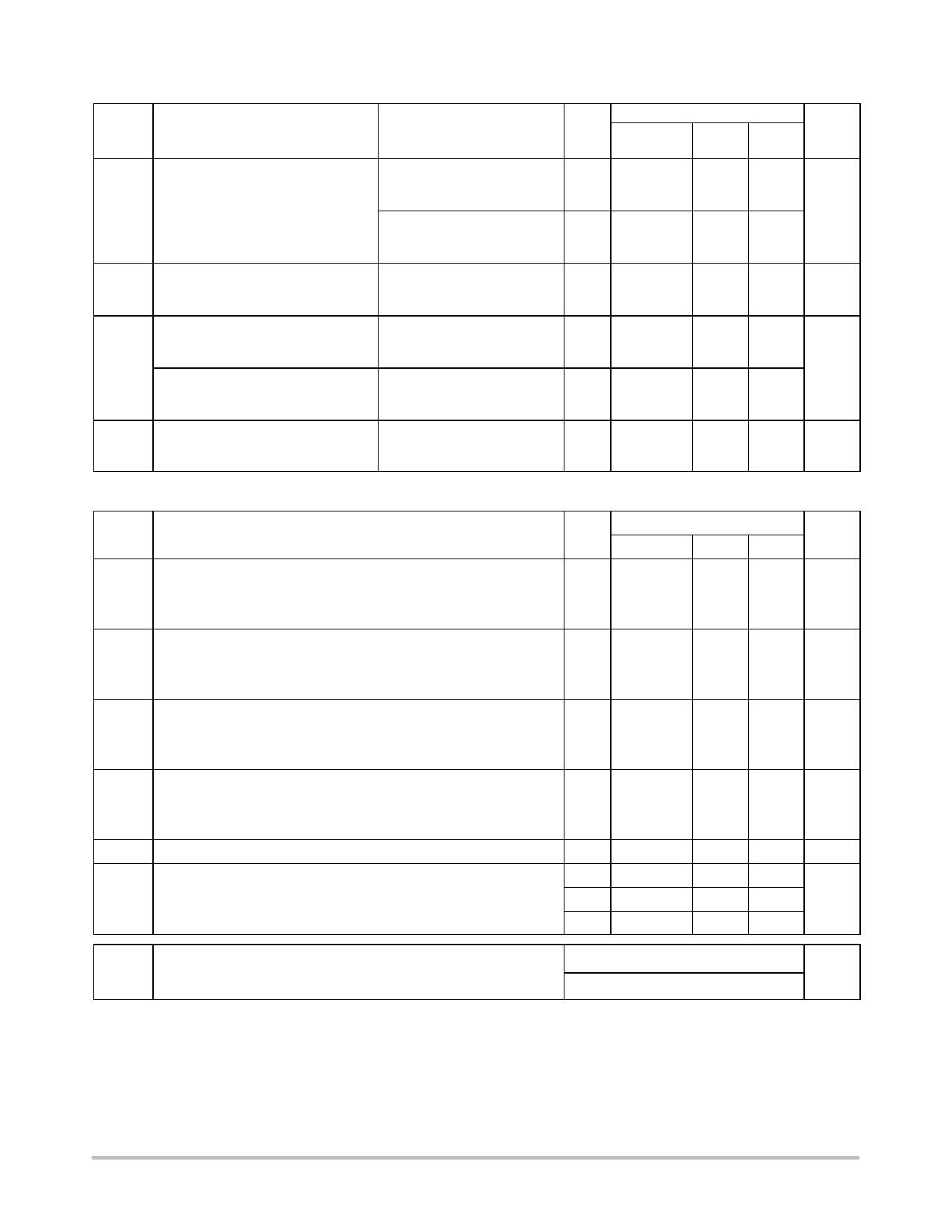
DC ELECTRICAL CHARACTERISTICS Analog Section
Guaranteed Limit
ÎÎÎÎÎÎÎÎÎÎÎÎÎÎÎÎÎÎÎÎÎÎÎÎÎÎÎÎÎÎÎÎÎÎÎÎÎÎÎÎÎÎÎÎÎÎÎÎÎÎÎÎÎÎÎÎÎÎÎÎÎÎÎÎÎÎ Symbol
Parameter
Test Conditions
VCC
v
v
V −55 to 25°C 85°C 125°C Unit
ÎÎÎÎÎÎÎÎÎÎÎÎÎÎÎÎÎÎÎÎÎÎÎÎÎÎÎÎÎÎÎÎÎÎÎÎÎÎÎÎÎÎÎÎÎÎÎÎÎÎÎÎÎÎÎÎÎÎÎÎÎÎÎÎÎÎ Ron Maximum“ON”Resistance
Vin = VIL or VIH
3.0
40
VIS = VCC to GND
4.5
30
|IS| v 10.0 mA (Figures 1, 2)
5.5
25
ÎÎÎÎÎÎÎÎÎÎÎÎÎÎÎÎÎÎÎÎÎÎÎÎÎÎÎÎÎÎÎÎÎ Vin = VIL or VIH
3.0
30
ÎÎÎÎÎÎÎÎÎÎÎÎÎÎÎÎÎÎÎÎÎÎÎÎÎÎÎÎÎÎÎÎÎ VIS = VCC or GND (Endpoints) 4.5
25
|IS| v 10.0 mA (Figures 1, 2)
5.5
20
ÎÎÎÎÎÎÎÎÎÎÎÎÎÎÎÎÎÎÎÎÎÎÎÎÎÎÎÎÎÎÎÎÎÎÎÎÎÎÎÎÎÎÎÎÎÎÎÎÎÎÎÎÎÎÎÎÎÎÎÎÎÎÎÎÎÎÎÎÎÎÎÎÎÎÎÎÎÎÎÎÎÎÎÎÎÎÎÎÎÎÎÎÎÎÎÎÎÎÎ DRon
Maximum Difference in “ON”
Resistance Between Any Two
Channels in the Same Package
Vin = VIL or VIH
VIS = 1/2 (VCC − GND)
|IS| v 10.0 mA
3.0
15
4.5
8.0
5.5
8.0
ÎÎÎÎÎÎÎÎÎÎÎÎÎÎÎÎÎÎÎÎÎÎÎÎÎÎÎÎÎÎÎÎÎ Ioff Maximum Off−Channel Leakage
Vin = VIL or VIH;
5.5
0.1
45
50
W
32
37
28
30
35
40
28
35
25
30
20
25
W
12
15
12
15
0.5
1.0
mA
Current, Any One Channel
VIO = VCC or GND;
Switch Off (Figure 3)
Maximum Off−Channel
Leakage Current,
Common Channel
Vin = VIL or VIH;
VIO = VCC or GND;
Switch Off (Figure 4)
5.5
0.1
1.0
2.0
Ion Maximum On−Channel
Leakage Current,
Channel−to−Channel
Vin = VIL or VIH;
Switch−to−Switch =
VCC or GND; (Figure 5)
5.5
0.1
1.0
2.0
mA
AC CHARACTERISTICS (CL = 50 pF, Input tr = tf = 3 ns)
Symbol
Parameter
tPLH,
tPHL
Maximum Propagation Delay, Channel−Select to Analog Output
(Figure 9)
tPLH,
tPHL
Maximum Propagation Delay, Analog Input to Analog Output
(Figure 10)
tPLZ,
tPHZ
Maximum Propagation Delay, Enable to Analog Output
(Figure 11)
tPZL,
tPZH
Maximum Propagation Delay, Enable to Analog Output
(Figure 11)
Cin Maximum Input Capacitance, Channel−Select or Enable Inputs
CI/O Maximum Capacitance
Analog I/O
(All Switches Off)
Common O/I
Feedthrough
Guaranteed Limit
VCC
V −55 to 25°C ≤85°C ≤125°C Unit
2.0
30
3.0
20
4.5
15
5.5
15
35
40
ns
25
30
18
22
18
20
2.0
4.0
3.0
3.0
4.5
1.0
5.5
1.0
6.0
8.0
ns
5.0
6.0
2.0
2.0
2.0
2.0
2.0
30
3.0
20
4.5
15
5.5
15
35
40
ns
25
30
18
22
18
20
2.0
20
3.0
12
4.5
8.0
5.5
8.0
25
30
ns
14
15
10
12
10
12
10
10
10
pF
35
35
35
pF
50
50
50
1.0
1.0
1.0
Typical @ 25°C, VCC = 5.0 V
CPD Power Dissipation Capacitance (Figure 13)*
45
pF
* Used to determine the no−load dynamic power consumption: PD = CPD VCC2f + ICC VCC.
http://onsemi.com
4
Share Link: 