MC74LVX4052DG(2011) 데이터 시트보기 (PDF) - ON Semiconductor
부품명
상세내역
일치하는 목록
MC74LVX4052DG Datasheet PDF : 15 Pages
| |||
MC74LVX4052
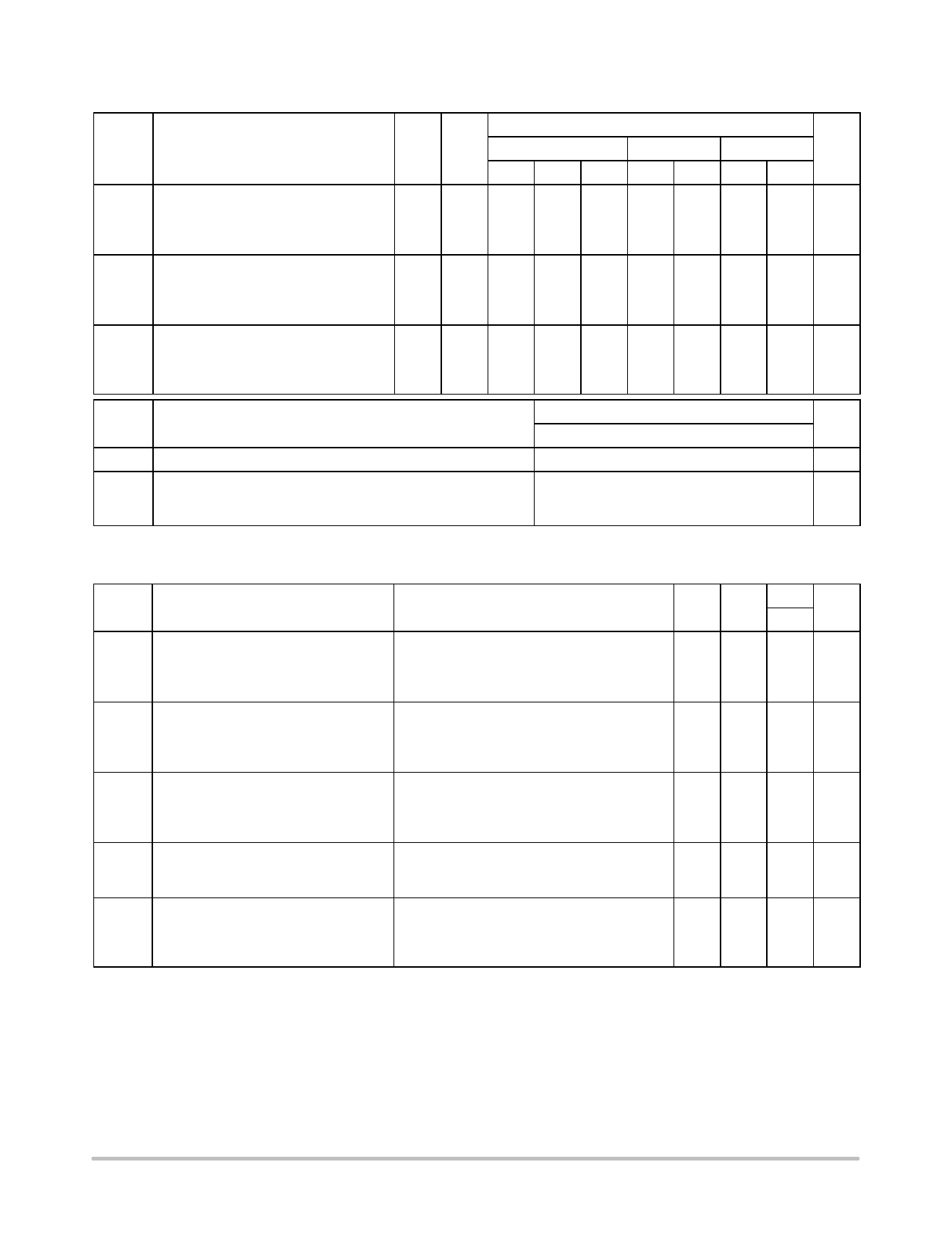
AC CHARACTERISTICS (CL = 50 pF, Input tr = tf = 3 ns)
Symbol
tPLH,
tPHL
Parameter
Maximum Propagation Delay,
Channel−Select to Analog Output
(Figures 16 and 17)
tPLZ,
tPHZ
Maximum Propagation Delay, Enable to
Analog Output (Figures 14 and 15)
tPZL,
tPZH
Maximum Propagation Delay, Enable to
Analog Output (Figures 14 and 15)
Guaranteed Limit
VCC VEE
*55 to 25°C
v85°C
v125°C
V
V
Min Typ Max Min Max Min Max Unit
2.5
0
3.0
0
4.5
0
3.0 *3.0
40
45
50
ns
28
30
35
23
25
30
23
25
28
2.5
0
3.0
0
4.5
0
3.0 *3.0
40
45
50
ns
28
30
35
23
25
30
23
25
28
2.5
0
3.0
0
4.5
0
3.0 *3.0
40
45
50
ns
28
30
35
23
25
30
23
25
28
Typical @ 25°C, VCC = 5.0 V, VEE = 0V
CPD Power Dissipation Capacitance (Figure 18) (Note 6)
45
pF
CIN Maximum Input Capacitance, Channel−Select or Enable Inputs
10
pF
CI/O Maximum Capacitance
(All Switches Off)
Analog I/O
10
Common O/I
10
Feedthrough
1.0
pF
6. Used to determine the no−load dynamic power consumption: PD = CPD VCC2f + ICC VCC.
ADDITIONAL APPLICATION CHARACTERISTICS (GND = 0 V)
Symbol
Parameter
BW Maximum On−Channel Bandwidth or
Minimum Frequency Response
VISO Off−Channel Feedthrough Isolation
VONL Maximum Feedthrough On Loss
Q Charge Injection
THD Total Harmonic Distortion THD + Noise
Condition
VIS = ½ (VCC − VEE)
Ref and Test Attn = 10 dB
Source Amplitude = 0 dB
(Figure 7)
f = 1 MHz; VIS = ½ (VCC − VEE)
Adjust Network Analyzer output to 10 dBm on
each output from the power splitter
(Figures 8 and 9)
VIS = ½ (VCC − VEE)
Adjust Network Analyzer output to 10 dBm on
each output from the power splitter
(Figure 11)
VIN = VCC to VEE, fIS = 1 kHz, tr = tf = 3 ns
RIS = 0 W, CL= 1000 pF, Q = CL * ΔVOUT
(Figure 10)
fIS = 1 MHz, RL = 10 KW, CL = 50 pF,
VIS = 5.0 VPP sine wave
VIS = 6.0 VPP sine wave
(Figure 19)
Typ
VCC VEE
V
V 25°C Unit
3.0 0.0 80
4.5 0.0 80
6.0 0.0 80
3.0 *3.0 80
MHz
3.0 0.0 *70 dB
4.5 0.0 *70
6.0 0.0 *70
3.0 *3.0 *70
3.0 0.0 *2 dB
4.5 0.0 *2
6.0 0.0 *2
3.0 *3.0 *2
5.0 0.0 9.0 pC
3.0 *3.0 12
%
6.0 0.0 0.10
3.0 *3.0 0.05
http://onsemi.com
5
Share Link: 