MC74HCT273A 데이터 시트보기 (PDF) - ON Semiconductor
부품명
상세내역
일치하는 목록
MC74HCT273A
ON Semiconductor

MC74HCT273A Datasheet PDF : 7 Pages
| |||
MC74HCT273A
Octal D Flip-Flop with
Common Clock and Reset
with LSTTL-Compatible
Inputs
High−Performance Silicon−Gate CMOS
The MC74HCT273A may be used as a level converter for
interfacing TTL or NMOS outputs to High−Speed CMOS inputs.
The HCT273A is identical in pinout to the LS273.
This device consists of eight D flip−flops with common Clock and
Reset inputs. Each flip−flop is loaded with a low−to−high transition of
the Clock input. Reset is asynchronous and active low.
Features
• Output Drive Capability: 10 LSTTL Loads
• TTL/NMOS Compatible Input Levels
• Outputs Directly Interface to CMOS, NMOS and TTL
• Operating Voltage Range: 4.5 V to 5.5 V
• Low Input Current: 1.0 μA
• In Compliance with the Requirements Defined by JEDEC Standard
No. 7 A
• Chip Complexity: 284 FETs or 71 Equivalent Gates
• These Devices are Pb−Free and are RoHS Compliant
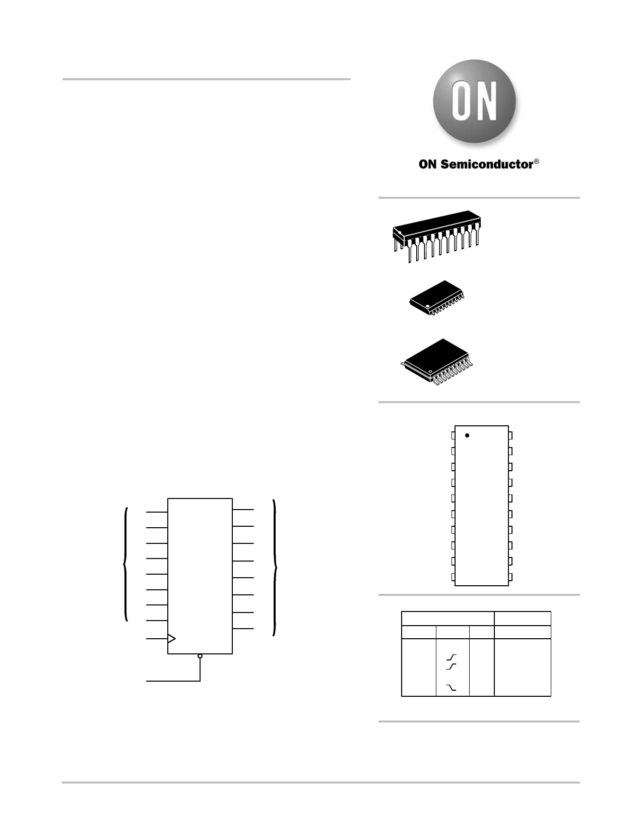
DATA
INPUTS
D0 3
D1 4
D2 7
D3 8
D4 13
D5 14
D6 17
D7 18
CLOCK 11
2 Q0
5 Q1
6 Q2
9 Q3
12 Q4
15 Q5
16 Q6
19 Q7
NONINVERTING
OUTPUTS
RESET 1
PIN 20 = VCC
PIN 10 = GND
Figure 1. Logic Diagram
© Semiconductor Components Industries, LLC, 2011
1
May, 2011 − Rev. 11
http://onsemi.com
1
1
PDIP−20
N SUFFIX
CASE 738
SOIC−20W
DW SUFFIX
CASE 751D
TSSOP−20
DT SUFFIX
CASE 948E
1
PIN ASSIGNMENT
RESET 1
Q0 2
D0 3
D1 4
Q1 5
Q2 6
D2 7
D3 8
Q3 9
GND 10
20 VCC
19 Q7
18 D7
17 D6
16 Q6
15 Q5
14 D5
13 D4
12 Q4
11 CLOCK
FUNCTION TABLE
Inputs
Output
Reset Clock D
Q
L
X
X
L
H
H
H
H
L
L
H
L
X No Change
H
X No Change
X = Don’t Care
Z = High Impedance
ORDERING INFORMATION
See detailed ordering, shipping information, and marking
information in the package dimensions section on page 5 of
this data sheet.
Publication Order Number:
MC74HCT273A/D
Share Link: