MC74HCT14AN 데이터 시트보기 (PDF) - ON Semiconductor
부품명
상세내역
일치하는 목록
MC74HCT14AN Datasheet PDF : 8 Pages
| |||
MC74HCT14A
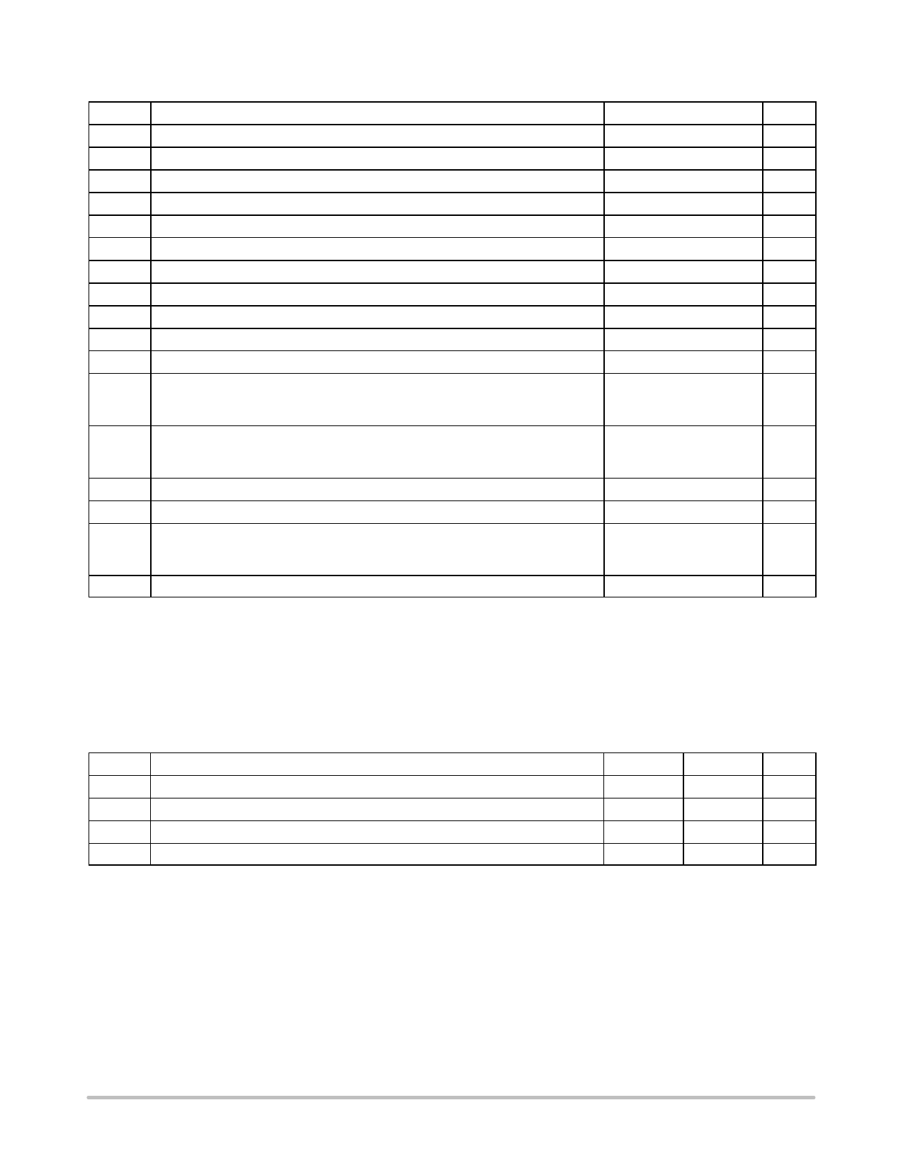
MAXIMUM RATINGS (Note 1)
Symbol
Parameter
Value
Unit
VCC
VI
VO
IIK
IOK
IO
ICC
IGND
TSTG
TL
TJ
qJA
DC Supply Voltage
DC Input Voltage
DC Output Voltage
DC Input Diode Current
DC Output Diode Current
DC Output Sink Current
DC Supply Current per Supply Pin
DC Ground Current per Ground Pin
Storage Temperature Range
Lead Temperature, 1 mm from Case for 10 Seconds
Junction Temperature under Bias
Thermal Resistance
(Referenced to GND)
(Referenced to GND)
(Referenced to GND)
PDIP
SOIC
TSSOP
*0.5 to )7.0
*0.5 to VCC )0.5
*0.5 to VCC )0.5
$20
$25
$25
$50
$50
*65 to )150
260
)150
78
125
170
V
V
V
mA
mA
mA
mA
mA
_C
_C
_C
_C/W
PD
Power Dissipation in Still Air at 85_C
PDIP
750
mW
SOIC
500
TSSOP
450
MSL
Moisture Sensitivity
Level 1
FR
VESD
Flammability Rating
ESD Withstand Voltage
Oxygen Index: 30% - 35%
UL-94-VO (0.125 in)
Human Body Model (Note 2)
>4000
V
Machine Model (Note 3)
>300
Charged Device Model (Note 4)
>1000
ILatch- Up Latch-Up Performance
Above VCC and Below GND at 85_C (Note 5)
$300
mA
1. Absolute maximum continuous ratings are those values beyond which damage to the device may occur. Extended exposure to these
conditions or conditions beyond those indicated may adversely affect device reliability. Functional operation under absolute maximum-rated
conditions is not implied.
2. Tested to EIA/JESD22-A114-A.
3. Tested to EIA/JESD22-A115-A.
4. Tested to JESD22-C101-A.
5. Tested to EIA/JESD78.
6. For high frequency or heavy load considerations, see the ON Semiconductor High- Speed CMOS Data Book (DL129/D).
RECOMMENDED OPERATING CONDITIONS
Symbol
Parameter
ÎÎÎÎÎÎÎÎÎÎÎÎÎÎÎÎÎÎÎÎÎÎÎÎÎÎÎÎÎÎÎÎÎ VCC
ÎÎÎÎÎÎÎÎÎÎÎÎÎÎÎÎÎÎÎÎÎÎÎÎÎÎÎÎÎÎÎÎÎ VI, VO
ÎÎÎÎÎÎÎÎÎÎÎÎÎÎÎÎÎÎÎÎÎÎÎÎÎÎÎÎÎÎÎÎÎ TA
ÎÎÎÎÎÎÎÎÎÎÎÎÎÎÎÎÎÎÎÎÎÎÎÎÎÎÎÎÎÎÎÎÎ tr, tf
DC Supply Voltage
DC Input Voltage, Output Voltage
Operating Temperature, All Package Types
Input Rise and Fall Time (Figure 3)
ÎÎÎÎÎÎÎÎÎÎÎÎÎÎÎÎÎÎÎÎÎÎÎÎÎÎÎÎÎÎÎÎÎ 7. No Limit when VI [ 50% VCC, ICC > 1 mA.
(Referenced to GND)
(Referenced to GND)
Min
4.5
0
*55
—
Max
Unit
5.5
V
VCC
V
)125
_C
(Note 7)
ns
8. Unused inputs may not be left open. All inputs must be tied to a high-logic voltage level or a low-logic input voltage level.
http://onsemi.com
3
Share Link: 