MC74HC390ADTR2 데이터 시트보기 (PDF) - ON Semiconductor
부품명
상세내역
일치하는 목록
MC74HC390ADTR2 Datasheet PDF : 10 Pages
| |||
MC74HC390A
TIMING REQUIREMENTS (Input tr = tf = 6 ns)
ÎÎÎÎÎÎÎÎÎÎÎÎÎÎÎÎÎÎÎÎÎÎÎÎÎÎÎÎÎÎÎÎÎÎÎÎÎÎÎÎÎÎÎÎÎÎÎÎÎÎÎÎÎÎÎÎÎÎÎÎÎÎÎÎÎÎ Symbol
ÎÎÎÎÎÎÎÎÎÎÎÎÎÎÎÎÎÎÎÎÎÎÎÎÎÎÎÎÎÎÎÎÎÎÎÎÎÎÎÎÎÎÎÎÎÎÎÎÎÎÎÎÎÎÎÎÎÎÎÎÎÎÎÎÎÎ trec
Parameter
Minimum Recovery Time, Reset Inactive to Clock A or Clock B
(Figure 2)
ÎÎÎÎÎÎÎÎÎÎÎÎÎÎÎÎÎÎÎÎÎÎÎÎÎÎÎÎÎÎÎÎÎÎÎÎÎÎÎÎÎÎÎÎÎÎÎÎÎÎÎÎÎÎÎÎÎÎÎÎÎÎÎÎÎÎ tw
Minimum Pulse Width, Clock A, Clock B
ÎÎÎÎÎÎÎÎÎÎÎÎÎÎÎÎÎÎÎÎÎÎÎÎÎÎÎÎÎÎÎÎÎ (Figure 1)
ÎÎÎÎÎÎÎÎÎÎÎÎÎÎÎÎÎÎÎÎÎÎÎÎÎÎÎÎÎÎÎÎÎÎÎÎÎÎÎÎÎÎÎÎÎÎÎÎÎÎÎÎÎÎÎÎÎÎÎÎÎÎÎÎÎÎ tw
Minimum Pulse Width, Reset
ÎÎÎÎÎÎÎÎÎÎÎÎÎÎÎÎÎÎÎÎÎÎÎÎÎÎÎÎÎÎÎÎÎ (Figure 2)
ÎÎÎÎÎÎÎÎÎÎÎÎÎÎÎÎÎÎÎÎÎÎÎÎÎÎÎÎÎÎÎÎÎÎÎÎÎÎÎÎÎÎÎÎÎÎÎÎÎÎÎÎÎÎÎÎÎÎÎÎÎÎÎÎÎÎ tf, tf Maximum Input Rise and Fall Times
ÎÎÎÎÎÎÎÎÎÎÎÎÎÎÎÎÎÎÎÎÎÎÎÎÎÎÎÎÎÎÎÎÎÎÎÎÎÎÎÎÎÎÎÎÎÎÎÎÎÎÎÎÎÎÎÎÎÎÎÎÎÎÎÎÎÎÎÎÎÎÎÎÎÎÎÎÎÎÎÎÎÎÎÎÎÎÎÎÎÎÎÎÎÎÎÎÎÎÎ (Figure 1)
Guaranteed Limit
VCC
– 55 to
V
25_C v 85_C v 125_C Unit
2.0
25
30
40
ns
3.0
15
20
30
4.5
10
13
15
6.0
9
11
13
2.0
75
3.0
27
4.5
15
6.0
13
95
110
ns
32
36
19
22
15
19
2.0
75
3.0
27
4.5
20
6.0
18
95
110
ns
32
36
24
30
22
28
2.0
1000
1000
1000
ns
3.0
800
800
800
4.5
500
500
500
6.0
400
400
400
NOTE: Information on typical parametric values can be found in Chapter 2 of the ON Semiconductor High−Speed CMOS Data Book
(DL129/D).
PIN DESCRIPTIONS
INPUTS
Clock A (Pins 1, 15) and Clock B (Pins 4, 15)
Clock A is the clock input to the ÷ 2 counter; Clock B is
the clock input to the ÷ 5 counter. The internal flip−flops are
toggled by high−to−low transitions of the clock input.
CONTROL INPUTS
Reset (Pins 2, 14)
Asynchronous reset. A high at the Reset input prevents
counting, resets the internal flip−flops, and forces QA
through QD low.
OUTPUTS
QA (Pins 3, 13)
Output of the ÷ 2 counter.
QB, QC, QD (Pins 5, 6, 7, 9, 10, 11)
Outputs of the ÷ 5 counter. QD is the most significant bit.
QA is the least significant bit when the counter is connected
for BCD output as in Figure 4. QB is the least significant bit
when the counter is operating in the bi−quinary mode as in
Figure 5.
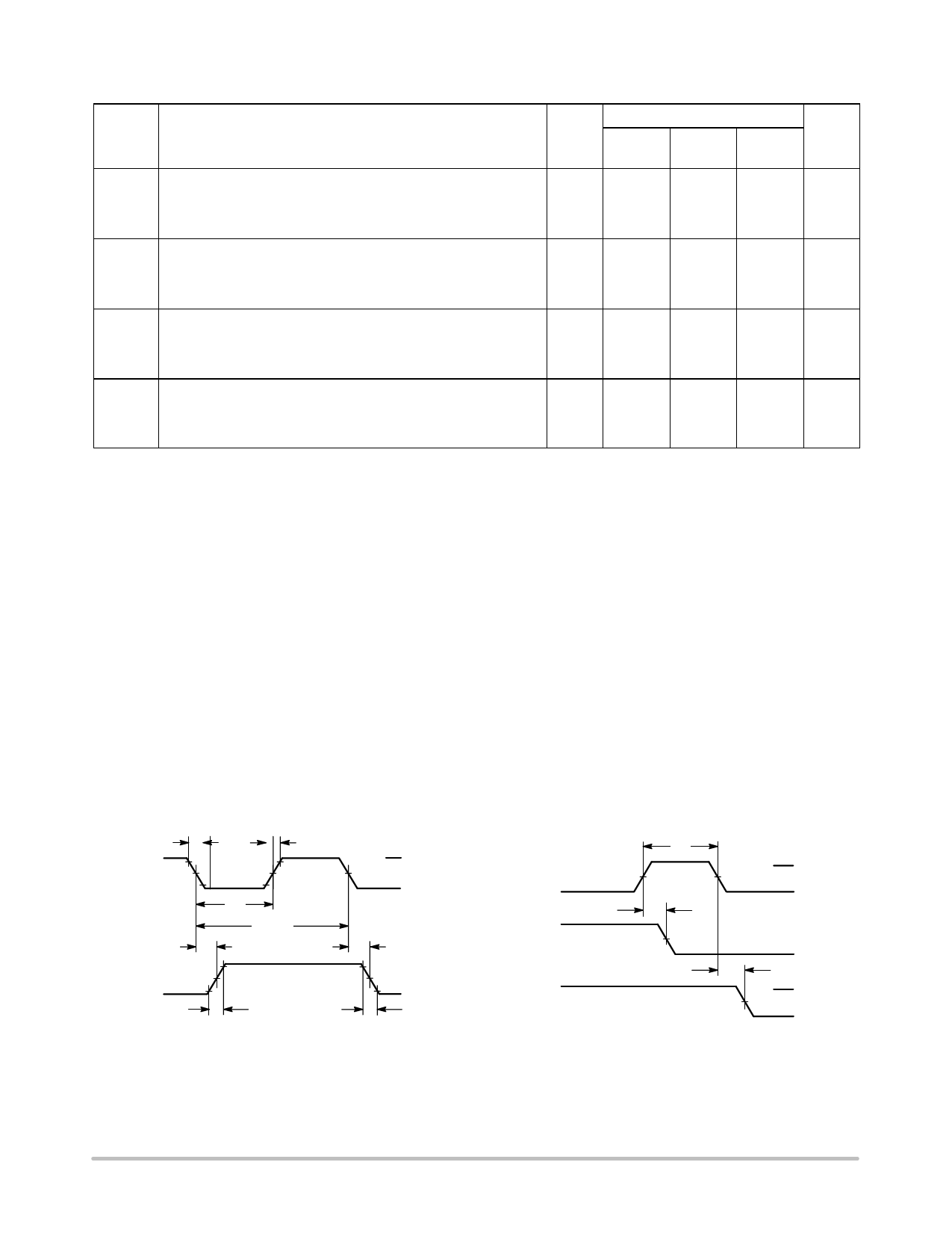
SWITCHING WAVEFORMS
tf
tr
90%
VCC
CLOCK
50%
10% 10%
GND
tw
1/fmax
tPLH
tPHL
90%
Q
50%
10%
tTLH
tTHL
Figure 3.
tw
VCC
RESET
50%
GND
tPHL
Q
50%
CLOCK
trec
VCC
50%
GND
Figure 4.
http://onsemi.com
5
Share Link: 