MC74HC365 데이터 시트보기 (PDF) - Motorola => Freescale
부품명
상세내역
일치하는 목록
MC74HC365 Datasheet PDF : 6 Pages
| |||
MC54/74HC365
ÎÎÎÎÎÎÎÎÎÎÎÎÎÎÎÎÎÎÎÎÎÎÎÎÎÎÎÎÎÎÎÎÎÎÎÎÎÎÎÎÎÎÎÎÎÎÎÎÎÎÎÎÎÎÎÎÎÎÎÎÎÎÎÎÎÎ DC ELECTRICAL CHARACTERISTICS (Voltages Referenced to GND)
ÎÎÎÎÎÎÎÎÎÎÎÎÎÎÎÎÎÎÎÎÎÎÎÎÎÎÎÎÎÎÎÎÎ Guaranteed Limit
ÎÎÎÎÎÎÎÎÎÎÎÎÎÎÎÎÎÎÎÎÎÎÎÎÎÎÎÎÎÎÎÎÎÎÎÎÎÎÎÎÎÎÎÎÎÎÎÎÎÎÎÎÎÎÎÎÎÎÎÎÎÎÎÎÎÎ Symbol
Parameter
Test Conditions
VCC
V
– 55 to
25_C
v v 85_C
125_C Unit
ÎÎÎÎÎÎÎÎÎÎÎÎÎÎÎÎÎÎÎÎÎÎÎÎÎÎÎÎÎÎÎÎÎ IOZ
Maximum Three–State
ÎÎÎÎÎÎÎÎÎÎÎÎÎÎÎÎÎÎÎÎÎÎÎÎÎÎÎÎÎÎÎÎÎ Leakage Current
Output in High–Impedance State
6.0
± 0.5
± 5.0
± 10
µA
Vin = VIL or VIH
Vout = VCC or GND
ÎÎÎÎÎÎÎÎÎÎÎÎÎÎÎÎÎÎÎÎÎÎÎÎÎÎÎÎÎÎÎÎÎ ICC
Maximum Quiescent Supply
ÎÎÎÎÎÎÎÎÎÎÎÎÎÎÎÎÎÎÎÎÎÎÎÎÎÎÎÎÎÎÎÎÎ Current (per Package)
Vin = VCC or GND
Iout = 0 µA
6.0
8
80
160
µA
ÎÎÎÎÎÎÎÎÎÎÎÎÎÎÎÎÎÎÎÎÎÎÎÎÎÎÎÎÎÎÎÎÎ NOTE: Information on typical parametric values can be found in Chapter 2 of the Motorola High–Speed CMOS Data Book (DL129/D).
ÎÎÎÎÎÎÎÎÎÎÎÎÎÎÎÎÎÎÎÎÎÎÎÎÎÎÎÎÎÎÎÎÎ AC ELECTRICAL CHARACTERISTICS (CL = 50 pF, Input tr = tf = 6 ns)
ÎÎÎÎÎÎÎÎÎÎÎÎÎÎÎÎÎÎÎÎÎÎÎÎÎÎÎÎÎÎÎÎÎÎÎÎÎÎÎÎÎÎÎÎÎÎÎÎÎÎÎÎÎÎÎÎÎÎÎÎÎÎÎÎÎÎÎÎÎÎÎÎÎÎÎÎÎÎÎÎÎÎÎÎÎÎÎÎÎÎÎÎÎÎÎÎÎÎÎ Symbol
ÎÎÎÎÎÎÎÎÎÎÎÎÎÎÎÎÎÎÎÎÎÎÎÎÎÎÎÎÎÎÎÎÎ tPLH,
ÎÎÎÎÎÎÎÎÎÎÎÎÎÎÎÎÎÎÎÎÎÎÎÎÎÎÎÎÎÎÎÎÎ tPHL
Parameter
Maximum Propagation Delay, Input A to Output Y
(Figures 1 and 3)
ÎÎÎÎÎÎÎÎÎÎÎÎÎÎÎÎÎÎÎÎÎÎÎÎÎÎÎÎÎÎÎÎÎ tPLZ,
ÎÎÎÎÎÎÎÎÎÎÎÎÎÎÎÎÎÎÎÎÎÎÎÎÎÎÎÎÎÎÎÎÎ tPHZ
Maximum Propagation Delay, Output Enable to Output Y
(Figures 2 and 4)
ÎÎÎÎÎÎÎÎÎÎÎÎÎÎÎÎÎÎÎÎÎÎÎÎÎÎÎÎÎÎÎÎÎÎÎÎÎÎÎÎÎÎÎÎÎÎÎÎÎÎÎÎÎÎÎÎÎÎÎÎÎÎÎÎÎÎ tPZL,
tPZH
Maximum Propagation Delay, Output Enable to Output Y
(Figures 2 and 4)
ÎÎÎÎÎÎÎÎÎÎÎÎÎÎÎÎÎÎÎÎÎÎÎÎÎÎÎÎÎÎÎÎÎÎÎÎÎÎÎÎÎÎÎÎÎÎÎÎÎÎÎÎÎÎÎÎÎÎÎÎÎÎÎÎÎÎ tTLH,
tTHL
Maximum Output Transition Time, Any Output
(Figures 1 and 3)
ÎÎÎÎÎÎÎÎÎÎÎÎÎÎÎÎÎÎÎÎÎÎÎÎÎÎÎÎÎÎÎÎÎÎÎÎÎÎÎÎÎÎÎÎÎÎÎÎÎÎÎÎÎÎÎÎÎÎÎÎÎÎÎÎÎÎ Cin
ÎÎÎÎÎÎÎÎÎÎÎÎÎÎÎÎÎÎÎÎÎÎÎÎÎÎÎÎÎÎÎÎÎ Cout
ÎÎÎÎÎÎÎÎÎÎÎÎÎÎÎÎÎÎÎÎÎÎÎÎÎÎÎÎÎÎÎÎÎÎÎÎÎÎÎÎÎÎÎÎÎÎÎÎÎÎÎÎÎÎÎÎÎÎÎÎÎÎÎÎÎÎ NOTES:
Maximum Input Capacitance
Maximum Three–State Output Capacitance
(Output in High–Impedance State)
VCC
V
2.0
4.5
6.0
2.0
4.5
6.0
2.0
4.5
6.0
2.0
4.5
6.0
—
—
Guaranteed Limit
v v – 55 to
25_C
85_C
125_C Unit
120
150
180
ns
24
30
36
20
26
31
220
275
330
ns
44
55
66
37
47
56
220
275
330
ns
44
55
66
37
47
56
60
75
90
ns
12
15
18
10
13
15
10
10
10
pF
15
15
15
pF
1. For propagation delays with loads other than 50 pF, see Chapter 2 of the Motorola High–Speed CMOS Data Book (DL129/D).
2. Information on typical parametric values can be found in Chapter 2 of the Motorola High–Speed CMOS Data Book (DL129/D).
Typical @ 25°C, VCC = 5.0 V
CPD
Power Dissipation Capacitance (Per Buffer)*
40
pF
* Used to determine the no–load dynamic power consumption: PD = CPD VCC2f + ICC VCC. For load considerations, see Chapter 2 of the
Motorola High–Speed CMOS Data Book (DL129/D).
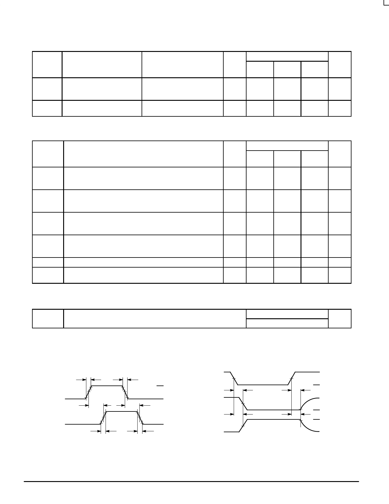
SWITCHING WAVEFORMS
tr
INPUT A
tPLH
OUTPUT Y
90%
50%
10%
90%
50%
10%
tTLH
Figure 1.
tf
VCC
GND
tPHL
tTHL
OUTPUT ENABLE
OUTPUT Y
OUTPUT Y
50%
tPZL tPLZ
50%
tPZH tPHZ
50%
Figure 2.
VCC
GND
HIGH
IMPEDANCE
10% VOL
90% VOH
HIGH
IMPEDANCE
High–Speed CMOS Logic Data
3
DL129 — Rev 6
MOTOROLA
Share Link: 