MC74HC299N 데이터 시트보기 (PDF) - Motorola => Freescale
부품명
상세내역
일치하는 목록
MC74HC299N Datasheet PDF : 8 Pages
| |||
MOTOROLA
SEMICONDUCTOR TECHNICAL DATA
8-Bit Bidirectional Universal
Shift Register with Parallel I/O
High–Performance Silicon–Gate CMOS
The MC74HC299 is identical in pinout to the LS299. The device inputs are
compatible with standard CMOS outputs; with pullup resistors, they are
compatible with LSTTL outputs.
The HC299 features a multiplexed parallel input/output data port to
achieve full 8–bit handling in a 20 pin package. Due to the large output drive
capability and the 3–state feature, this device is ideally suited for interface
with bus lines in a bus–oriented system.
Two Mode–Select inputs and two Output Enable inputs are used to
choose the mode of operation as listed in the Function Table. Synchronous
parallel loading is accomplished by taking both Mode–Select lines, S1 and
S2, high. This places the outputs in the high–impedance state, which permits
data applied to the data port to be clocked into the register. Reading out of
the register can be accomplished when the outputs are enabled. The
active–low asynchronous Reset overrides all other inputs.
• Output Drive Capability: 15 LSTTL Loads for QA through QH
10 LSTTL Loads for QA′ and QH′
• Outputs Directly Interface to CMOS, NMOS, and TTL
• Operating Voltage Range: 2 to 6 V
• Low Input Current: 1 µA
• High Noise Immunity Characteristic of CMOS Devices
• In Compliance with the Requirements Defined by JEDEC Standard
No. 7A
• Chip Complexity: 398 FETs or 99.5 Equivalent Gates
LOGIC DIAGRAM
SERIAL
DATA
INPUTS
SA (SHIFT RIGHT) 11
SH (SHIFT LEFT) 18
CLOCK 12
RESET 9
MODE
SELECT
OUTPUT
S1
S2
OE1
1
19
2
ENABLES OE2 3
7
13
6
14
5
15
4
16
8
17
PA/QA
PB/QB
PC/QC
PD/QD
PE/QE
PF/QF
PG/QG
PH/QH
QA′
QH′
3–STATE
PARALLEL DATA PORT
(INPUTS/OUTPUTS)
SERIAL DATA
OUTPUTS
PIN 20 = VCC
PIN 10 = GND
MC74HC299
20
1
20
1
N SUFFIX
PLASTIC PACKAGE
CASE 738–03
DW SUFFIX
SOIC PACKAGE
CASE 751D–04
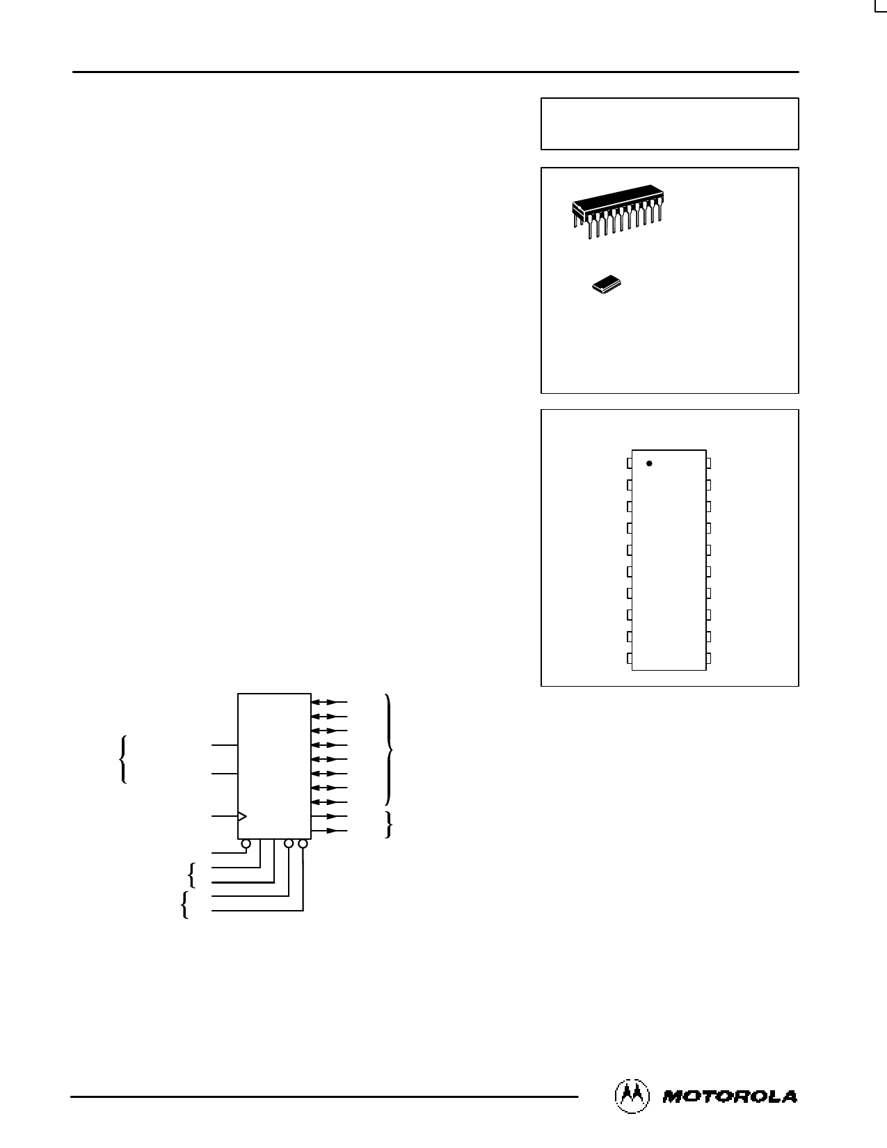
ORDERING INFORMATION
MC74HCXXXN
Plastic
MC74HCXXXDW SOIC
PIN ASSIGNMENT
S1 1
OE1 2
OE2 3
PG/QG 4
PE/QE 5
PC/QC 6
PA/QA 7
QA′ 8
RESET 9
GND 10
20 VCC
19 S2
18 SH
17 QH′
16 PH/QH
15 PF/QF
14 PD/QD
13 PB/QB
12 CLOCK
11 SA
10/95
© Motorola, Inc. 1995
3–1
REV 6
Share Link: 