74AC257 데이터 시트보기 (PDF) - ON Semiconductor
부품명
상세내역
일치하는 목록
74AC257 Datasheet PDF : 12 Pages
| |||
MC74AC257, MC74ACT257
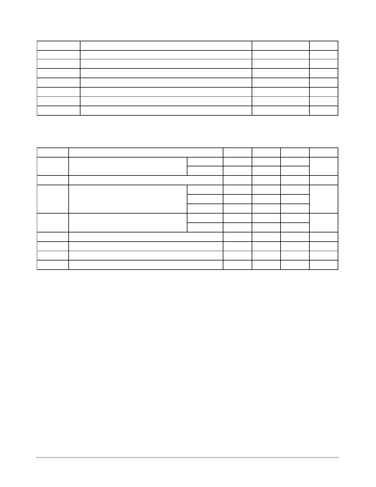
MAXIMUM RATINGS*
Symbol
Parameter
Value
Unit
VCC
VIN
VOUT
IIN
IOUT
ICC
Tstg
DC Supply Voltage (Referenced to GND)
DC Input Voltage (Referenced to GND)
DC Output Voltage (Referenced to GND)
DC Input Current, per Pin
DC Output Sink/Source Current, per Pin
DC VCC or GND Current per Output Pin
Storage Temperature
−0.5 to +7.0
V
−0.5 to VCC +0.5
V
−0.5 to VCC +0.5
V
±20
mA
±50
mA
±50
mA
−65 to +150
°C
*Maximum Ratings are those values beyond which damage to the device may occur. Functional operation should be restricted to the Recom-
mended Operating Conditions.
RECOMMENDED OPERATING CONDITIONS
Symbol
Parameter
Min
Typ
Max
VCC
Supply Voltage
′AC
′ACT
2.0
5.0
6.0
4.5
5.0
5.5
VIN, VOUT DC Input Voltage, Output Voltage (Ref. to GND)
0
−
VCC
tr, tf
Input Rise and Fall Time (Note 1)
′AC Devices except Schmitt Inputs
VCC @ 3.0 V
−
150
−
VCC @ 4.5 V
−
40
−
VCC @ 5.5 V
−
25
−
tr, tf
Input Rise and Fall Time (Note 2)
′ACT Devices except Schmitt Inputs
VCC @ 4.5 V
−
10
−
VCC @ 5.5 V
−
8.0
−
TJ
Junction Temperature (PDIP)
−
−
140
TA
Operating Ambient Temperature Range
−40
25
85
IOH
Output Current − High
−
−
−24
IOL
Output Current − Low
−
−
24
1. 1. Vin from 30% to 70% VCC; see individual Data Sheets for devices that differ from the typical input rise and fall times.
2. 2. Vin from 0.8 V to 2.0 V; see individual Data Sheets for devices that differ from the typical input rise and fall times.
Unit
V
V
ns/V
ns/V
°C
°C
mA
mA
http://onsemi.com
4
Share Link: 