74ACT299 데이터 시트보기 (PDF) - ON Semiconductor
부품명
상세내역
일치하는 목록
74ACT299 Datasheet PDF : 12 Pages
| |||
MC74AC299, MC74ACT299
8−Input Universal Shift/
Storage Register with
Common Parallel I/O Pins
The MC74AC299/74ACT299 is an 8−bit universal shift/storage
register with 3−state outputs. Four modes of operation are possible:
hold (store), shift left, shift right and load data. The parallel load inputs
and flip−flop outputs are multiplexed to reduce the total number of
package pins. Additional outputs are provided for flip−flops Q0, Q7 to
allow easy serial cascading. A separate active LOW Master Reset is
used to reset the register.
• Common Parallel I/O for Reduced Pin Count
• Additional Serial Inputs and Outputs for Expansion
• Four Operating Modes: Shift Left, Shift Right, Load and Store
• 3−State Outputs for Bus−Oriented Applications
• Outputs Source/Sink 24 mA
• ′ACT299 Has TTL Compatible Inputs
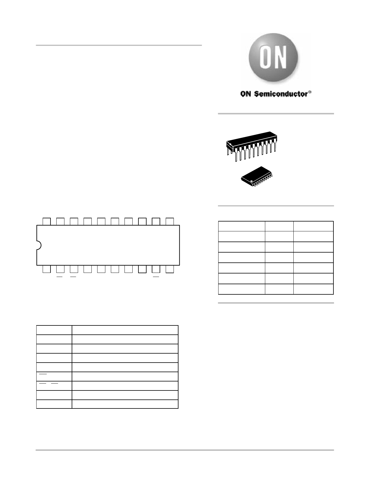
VCC S1 DS7 Q7 I/O7 I/O5 I/O3 I/O1 CP DS0
20 19 18 17 16 15 14 13 12 11
1 2 3 4 5 6 7 8 9 10
S0 OE1 OE2 I/O6 I/O4 I/O2 I/O0 Q0 MR GND
Figure 1. Pinout: 20−Lead Packages Conductors
(Top View)
PIN ASSIGNMENT
PIN
FUNCTION
CP
Clock Pulse Input
DS0
DS7
S0, S1
MR
Serial Data Input for Right Shift
Serial Data Input for Left Shift
Mode Select Inputs
Asynchronous Master Reset
OE1, OE2
I/O0−I/O7
Q0, Q7
3−State Output Enable Inputs
Parallel Data Inputs or 3−State Parallel Outputs
Serial Outputs
http://onsemi.com
20
1
20
1
PDIP−20
N SUFFIX
CASE 738
SO−20
DW SUFFIX
CASE 751
ORDERING INFORMATION
Device
Package
Shipping
MC74AC299N
PDIP−20 18 Units/Rail
MC74ACT299N
PDIP−20 18 Units/Rail
MC74AC299DW
SOIC−20 38 Units/Rail
MC74AC299DWR2 SOIC−20 1000 Tape & Reel
MC74ACT299DW SOIC−20 38 Units/Rail
MC74ACT299DWR2 SOIC−20 1000 Tape & Reel
DEVICE MARKING INFORMATION
See general marking information in the device marking
section on page 9 of this data sheet.
© Semiconductor Components Industries, LLC, 2003
1
April, 2003 − Rev. 6
Publication Order Number:
MC74AC299/D
Share Link: 