MC14049UB 데이터 시트보기 (PDF) - ON Semiconductor
부품명
상세내역
일치하는 목록
MC14049UB Datasheet PDF : 8 Pages
| |||
MC14049UB
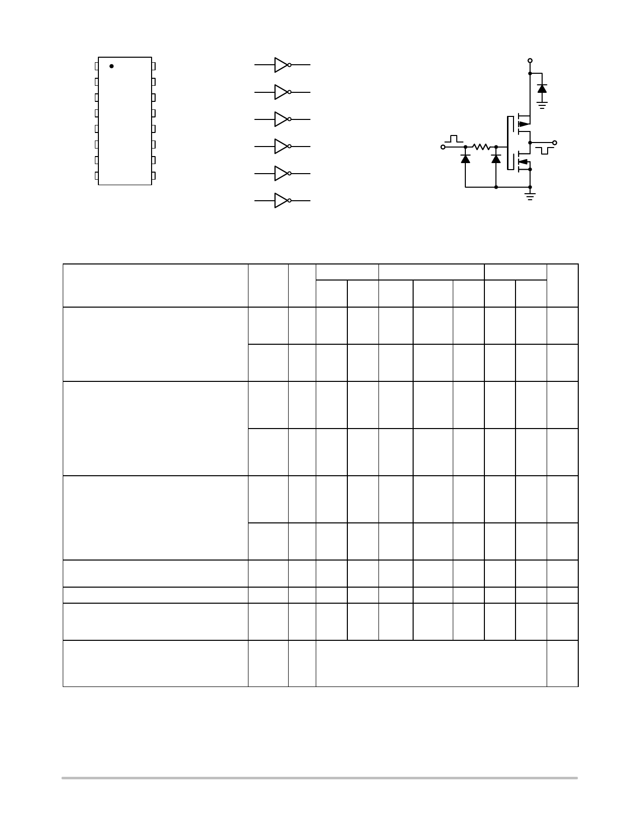
VDD 1
16 NC
3
2
VDD
OUTA 2
INA 3
15 OUTF
14 INF
5
4
MC14049UB
OUTB 4
INB 5
13 NC
12 OUTE
7
6
OUTC 6
11 INE
9
10
INC 7
10 OUTD
VSS 8
9 IND
11
12 NC = PIN 13, 16
VSS = PIN 8
NC = NO CONNECTION
14
15 VDD = PIN 1
VSS
Figure 1. Pin Assignment
Figure 2. Logic Diagram
Figure 3. Circuit Schematic
MC14049UB
(1/6 of circuit shown)
ÎÎÎÎÎÎÎÎÎÎÎÎÎÎÎÎÎÎÎÎÎÎÎÎÎÎÎÎÎÎÎÎÎ ELECTRICAL CHARACTERISTICS (Voltages Referenced to VSS)
ÎÎÎÎÎÎÎÎÎÎÎÎÎÎÎÎÎÎÎÎÎÎÎÎÎÎÎÎÎÎÎÎÎÎÎÎÎÎÎÎÎÎÎÎÎÎÎÎÎÎÎÎÎÎÎÎÎÎÎÎÎÎÎÎÎÎ Characteristic
Symbol
VDD
Vdc
− 55_C
Min Max
ÎÎÎÎÎÎÎÎÎÎÎÎÎÎÎÎÎÎÎÎÎÎÎÎÎÎÎÎÎÎÎÎÎ Output Voltage
ÎÎÎÎÎÎÎÎÎÎÎÎÎÎÎÎÎÎÎÎÎÎÎÎÎÎÎÎÎÎÎÎÎ Vin = VDD or 0
ÎÎÎÎÎÎÎÎÎÎÎÎÎÎÎÎÎÎÎÎÎÎÎÎÎÎÎÎÎÎÎÎÎÎÎÎÎÎÎÎÎÎÎÎÎÎÎÎÎÎÎÎÎÎÎÎÎÎÎÎÎÎÎÎÎÎ Vin = 0 or VDD
ÎÎÎÎÎÎÎÎÎÎÎÎÎÎÎÎÎÎÎÎÎÎÎÎÎÎÎÎÎÎÎÎÎÎÎÎÎÎÎÎÎÎÎÎÎÎÎÎÎÎÎÎÎÎÎÎÎÎÎÎÎÎÎÎÎÎ Input Voltage
ÎÎÎÎÎÎÎÎÎÎÎÎÎÎÎÎÎÎÎÎÎÎÎÎÎÎÎÎÎÎÎÎÎ (VO = 4.5 Vdc)
(VO = 9.0 Vdc)
ÎÎÎÎÎÎÎÎÎÎÎÎÎÎÎÎÎÎÎÎÎÎÎÎÎÎÎÎÎÎÎÎÎ (VO = 13.5 Vdc)
ÎÎÎÎÎÎÎÎÎÎÎÎÎÎÎÎÎÎÎÎÎÎÎÎÎÎÎÎÎÎÎÎÎÎÎÎÎÎÎÎÎÎÎÎÎÎÎÎÎÎÎÎÎÎÎÎÎÎÎÎÎÎÎÎÎÎ (VO = 0.5 Vdc)
(VO = 1.0 Vdc)
ÎÎÎÎÎÎÎÎÎÎÎÎÎÎÎÎÎÎÎÎÎÎÎÎÎÎÎÎÎÎÎÎÎ (VO = 1.5 Vdc)
ÎÎÎÎÎÎÎÎÎÎÎÎÎÎÎÎÎÎÎÎÎÎÎÎÎÎÎÎÎÎÎÎÎ Output Drive Current
ÎÎÎÎÎÎÎÎÎÎÎÎÎÎÎÎÎÎÎÎÎÎÎÎÎÎÎÎÎÎÎÎÎ (VOH = 2.5 Vdc)
(VOH = 9.5 Vdc)
ÎÎÎÎÎÎÎÎÎÎÎÎÎÎÎÎÎÎÎÎÎÎÎÎÎÎÎÎÎÎÎÎÎ (VOH = 13.5 Vdc)
ÎÎÎÎÎÎÎÎÎÎÎÎÎÎÎÎÎÎÎÎÎÎÎÎÎÎÎÎÎÎÎÎÎ (VOL = 0.4 Vdc)
ÎÎÎÎÎÎÎÎÎÎÎÎÎÎÎÎÎÎÎÎÎÎÎÎÎÎÎÎÎÎÎÎÎ (VOL = 0.5 Vdc)
(VOL = 1.5 Vdc)
ÎÎÎÎÎÎÎÎÎÎÎÎÎÎÎÎÎÎÎÎÎÎÎÎÎÎÎÎÎÎÎÎÎ Input Current
“0” Level
“1” Level
“0” Level
“1” Level
Source
Sink
VOL
5.0
−
0.05
10
− 0.05
15
− 0.05
VOH
5.0 4.95
−
10 9.95 −
15 14.95 −
VIL
5.0
−
1.0
10
−
2.0
15
−
2.5
VIH
5.0 4.0
−
10 8.0
−
15 12.5 −
IOH
5.0 – 1.6 −
10 – 1.6 −
15 – 4.7 −
IOL
5.0 3.75 −
10 10
−
15 30
−
Iin
15
− ± 0.1
ÎÎÎÎÎÎÎÎÎÎÎÎÎÎÎÎÎÎÎÎÎÎÎÎÎÎÎÎÎÎÎÎÎÎÎÎÎÎÎÎÎÎÎÎÎÎÎÎÎÎÎÎÎÎÎÎÎÎÎÎÎÎÎÎÎÎ Input Capacitance (Vin = 0)
ÎÎÎÎÎÎÎÎÎÎÎÎÎÎÎÎÎÎÎÎÎÎÎÎÎÎÎÎÎÎÎÎÎ Quiescent Current (Per Package)
ÎÎÎÎÎÎÎÎÎÎÎÎÎÎÎÎÎÎÎÎÎÎÎÎÎÎÎÎÎÎÎÎÎÎÎÎÎÎÎÎÎÎÎÎÎÎÎÎÎÎÎÎÎÎÎÎÎÎÎÎÎÎÎÎÎÎ Total Supply Current (Note 3 and 4)
ÎÎÎÎÎÎÎÎÎÎÎÎÎÎÎÎÎÎÎÎÎÎÎÎÎÎÎÎÎÎÎÎÎ (Dynamic plus Quiescent, Per Package)
ÎÎÎÎÎÎÎÎÎÎÎÎÎÎÎÎÎÎÎÎÎÎÎÎÎÎÎÎÎÎÎÎÎ (CL = 50 pF on all outputs, all buffers
ÎÎÎÎÎÎÎÎÎÎÎÎÎÎÎÎÎÎÎÎÎÎÎÎÎÎÎÎÎÎÎÎÎ switching)
Cin
−
−
−
IDD
5.0
−
1.0
10
−
2.0
15
−
4.0
IT
5.0
10
15
25_C
Min
Typ Max
(Note 2)
−
0
0.05
−
0
0.05
−
0
0.05
4.95
5.0
−
9.95
10
−
14.95
15
−
−
2.25
1.0
−
4.50
2.0
−
6.75
2.5
4.0
2.75
−
8.0
5.50
−
12.5 8.25
−
– 1.25 – 2.5
−
– 1.3 – 2.6
−
– 3.75 – 10
−
3.2
6.0
−
8.0
16
−
24
40
−
−
± 0.000 ± 0.1
01
−
10
20
−
0.002 1.0
−
0.004 2.0
−
0.006 4.0
IT = (1.8 mA/kHz) f + IDD
IT = (3.5 mA/kHz) f + IDD
IT = (5.3 mA/kHz) f + IDD
125_C
Min Max
− 0.05
− 0.05
− 0.05
4.95 −
9.95 −
14.95 −
−
1.0
−
2.0
−
2.5
4.0
−
8.0
−
12.5 −
– 1.0
– 1.0
– 3.0
2.6
6.6
19
−
−
−
−
−
−
−
± 1.0
−
−
−
30
−
60
−
120
Unit
Vdc
Vdc
Vdc
Vdc
mAdc
mAdc
mAdc
pF
mAdc
mAdc
2. Data labelled “Typ” is not to be used for design purposes but is intended as an indication of the IC’s potential performance.
3. The formulas given are for the typical characteristics only at 25_C.
4. To calculate total supply current at loads other than 50 pF:
IT(CL) = IT(50 pF) + (CL − 50) Vfk
where: IT is in mA (per package), CL in pF, V = (VDD − VSS) in volts, f in kHz is input frequency, and k = 0.002.
http://onsemi.com
2
Share Link: 