MB90860E 데이터 시트보기 (PDF) - Fujitsu
부품명
상세내역
일치하는 목록
MB90860E Datasheet PDF : 67 Pages
| |||
MB90860E Series
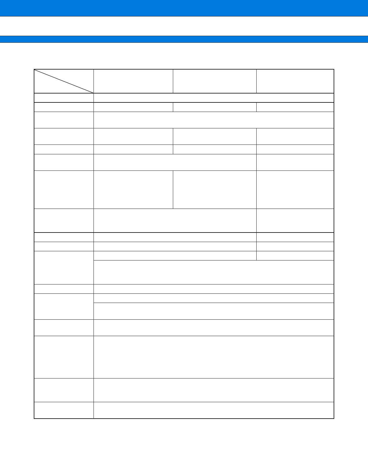
■ PRODUCT LINEUP
Part Number
Parameter
MB90867E(S)
MB90F867E(S)
MB90V340E-101/102
CPU
Type
System clock
ROM
RAM
Emulator-specific
power supply*1
Technology
Operating
voltage range
Temperature range
Package
UART
I2C (400 kbps)
8/10-bit
A/D converter
16-bit reload timer
(4 channels)
16-bit
I/O timer
(2 channels)
16-bit output
compare
(8 channels)
16-bit input capture
(8 channels)
F2MC-16LX CPU
MASK ROM product
Flash memory product
Evaluation product
On-chip PLL clock multiplier (×1, ×2, ×3, ×4, ×6, 1/2 when PLL stops)
Minimum instruction execution time : 42 ns (4 MHz osc. PLL × 6)
MASK ROM
128 Kbytes
Flash memory
128 Kbytes
External
6 Kbytes
6 Kbytes
30 Kbytes
⎯
Yes
0.35 µm CMOS with on-chip
voltage regulator for internal
power supply
0.35 µm CMOS with on-chip
voltage regulator for internal
power supply + Flash memory
with on-chip charge pump for
programming voltage
0.35 µm CMOS with on-chip
voltage regulator for internal
power supply
3.5 V to 5.5 V : at normal operating (not using A/D converter)
4.0 V to 5.5 V : at using A/D converter/Flash programming
4.5 V to 5.5 V : at using external bus
5 V ± 10%
−40 °C to +105 °C
⎯
QFP-100, LQFP-100
PGA-299
4 channels
5 channels
Wide range of baud rate settings using a dedicated reload timer
Special synchronous options for adapting to different synchronous serial protocols
LIN functionality working either as master or slave LIN device
2 channels
24 channels
10-bit or 8-bit resolution
Conversion time : Min 3 µs include sample time (per one channel)
Operation clock frequency : fsys/21, fsys/23, fsys/25 (fsys = Machine clock frequency)
Supports External Event Count function
Signals an interrupt when overflowing
Supports Timer Clear when a match with Output Compare (ch.0, ch.4)
Operation clock freq. : fsys, fsys/21, fsys/22, fsys/23, fsys/24, fsys/25, fsys/26, fsys/27
(fsys = Machine clock freq.)
I/O Timer 0 (clock input FRCK0) corresponds to ICU 0/1/2/3, OCU 0/1/2/3
I/O Timer 1 (clock input FRCK1) corresponds to ICU 4/5/6/7, OCU 4/5/6/7
Signals an interrupt when 16-bit I/O Timer match output compare registers.
A pair of compare registers can be used to generate an output signal.
Rising edge, falling edge or rising & falling edge sensitive
Signals an interrupt upon external event
(Continued)
4
Share Link: 