MB86616 데이터 시트보기 (PDF) - Fujitsu
부품명
상세내역
일치하는 목록
MB86616 Datasheet PDF : 63 Pages
| |||
MB86616
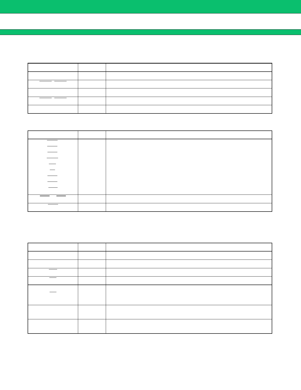
s PIN DESCRIPTION
1. IEEE 1394 Interface
Signal name
I/O
TPA0, TPA1
I/O
TPA0, TPA1
I/O
TPB0, TPB1
I/O
TPB0, TPB1
I/O
TPBIAS0, TPBIAS1
O
Function
TPA positive-signal input/output pin at IEEE 1394 port
TPA negative-signal input/output pin at IEEE 1394 port
TPB positive-signal input/output pin at IEEE 1394 port
TPB negative-signal input/output pin at IEEE 1394 port
Common-voltage reference voltage output pin at IEEE 1394 port
2. SCSI Interface
Signal name
I/O
Function
REQ,
ACK,
ATN,
MSG,
CD,
IO,
RST,
BSY,
SEL
I/O SCSI control signal input/output pins
DB0 to DB7
I/O Input/output pins for SCSI data bus
DBP
I/O Parity bit input/output pins for SCSI data bus
3. Internal CPU Pins (for Normal Operation Mode)
Note that the pin functions covered in this section are enabled only in the normal operation mode (with the
MODEA pin = “L”) .
Signal name
I/O
Function
A01 to A18
O
Address output pins
D00 to D15
I/O Data input pins
WR
O
Write strobe signal output pin
RD
O
Read strobe signal output pin
Pin to output the external flash ROM chip enable signal.
CS
O
This signal is output for accessing an address from F80000h to FFFFFFh in
memory space.
P74 to P76
P90 to P93
I/O General-purpose input/output port pins
MD0 to MD2
I
CPU block mode setting pins.
Connect all of these pins to GND on this device.
6
Share Link: 