MAX9737 데이터 시트보기 (PDF) - Maxim Integrated
부품명
상세내역
일치하는 목록
MAX9737 Datasheet PDF : 13 Pages
| |||

Mono 7W Class D Amplifier
ABSOLUTE MAXIMUM RATINGS
PVDD to PGND.......................................................-0.3V to +30V
AGND to PGND .....................................................-0.3V to +0.3V
IN, PRE, PC, COM to AGND.....................-0.3V to (VREG + 0.3V)
MUTE, SHDN to AGND ............................................-0.3V to +6V
REG to AGND ...............................................-0.3V to (VS + 0.3V)
VS to AGND ..............................................................-0.3V to +6V
OUT+, OUT- to PGND .............................-0.3V to (PVDD + 0.3V)
C1N to PGND ..........................................-0.3V to (PVDD + 0.3V)
C1P to PGND .........................(PVDD - 0.3V) to (VCHOLD + 0.3V)
CHOLD to PGND .......................................(VC1P - 0.3V) to +36V
OUT+, OUT-, Short Circuit to PGND or PVDD ...........Continuous
Thermal Limits (Notes 1, 2)
Continuous Power Dissipation (TA = +70°C)
24-Pin TQFN Single-Layer PCB (derate 20.8mW/°C
above +70°C)........................................................1666.7mW
θJA ................................................................................48°C/W
θJC..................................................................................3°C/W
Continuous Power Dissipation
24-Pin TQFN Multiple-Layer PCB
(derate 27.8mW/°C above +70°C) ........................2222.2mW
θJA ................................................................................36°C/W
θJC..................................................................................3°C/W
Operating Temperature Range ...........................-40°C to +85°C
Storage Temperature Range .............................-65°C to +150°C
Junction Temperature ......................................................+150°C
Lead Temperature (soldering, 10s) .................................+300°C
Note 1: Thermal performance of this device is highly dependent on PCB layout. See the Applications Information section for more detail.
Note 2: Package thermal resistances were obtained using the method described in JEDEC specification JESD51-7, using a four-layer
board. For detailed information on package thermal considerations, refer to www.maxim-ic.com/thermal-tutorial.
Stresses beyond those listed under “Absolute Maximum Ratings” may cause permanent damage to the device. These are stress ratings only, and functional
operation of the device at these or any other conditions beyond those indicated in the operational sections of the specifications is not implied. Exposure to
absolute maximum rating conditions for extended periods may affect device reliability.
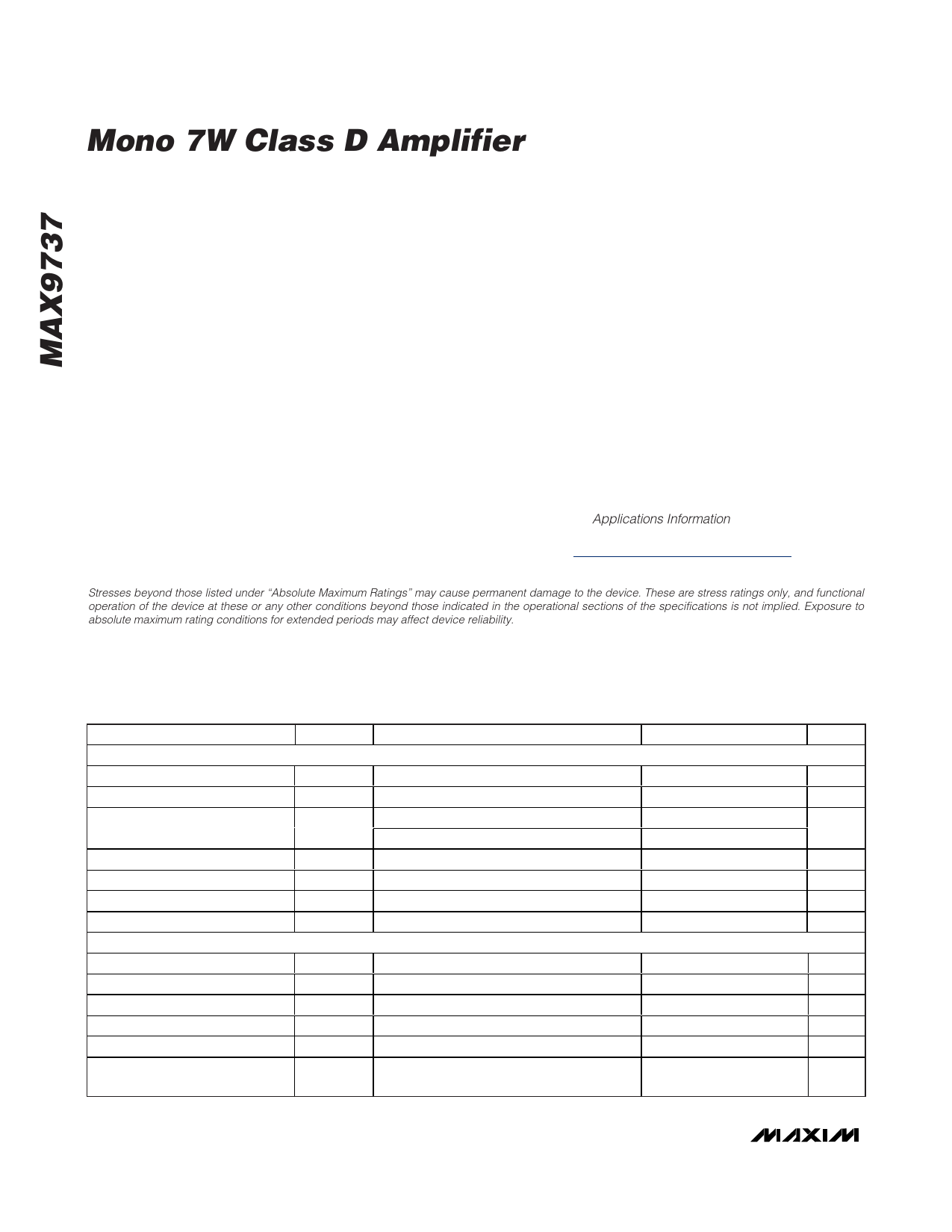
ELECTRICAL CHARACTERISTICS
(VPVDD = 12V, VAGND = VPGND = 0, VSHDN = VMUTE = 5V, C1 = 0.1µF, CIN = 0.47µF, C2 = CCOM = CREG = 1µF, RIN = RFB = 20kΩ,
RL = ∞, AC measurement bandwidth 22Hz to 22kHz, TA = TMIN to TMAX, unless otherwise noted. Typical values are at TA = +25°C.)
(Note 3)
PARAMETER
SYMBOL
AMPLIFIER DC CHARACTERISTICS
Speaker-Supply Voltage Range
PVDD
Undervoltage Lockout
UVLO
Quiescent Supply Current
IPVDD
CONDITIONS
Inferred from PSRR test
TA = +25°C
Shutdown Supply Current
ISHDN
REG Voltage
VREG
Preregulator Voltage
COM Voltage
VS
VCOM
INPUT AMPLIFIER CHARACTERISTICS
Capacitive Drive
CL
Output Swing
Open-Loop Gain
AVO
Input Offset Voltage
VOS
Input Amplifier Slew Rate
VSHDN = 0, TA = +25°C
No sustained oscillation
Sinking ±1mA (Note 4)
IN to COM
MIN TYP MAX UNITS
8
28
V
6.8
V
15
20
mA
25
1
10
µA
4.0
4.2
4.5
V
4.85
V
1.94 2.06 2.16
V
30
pF
2.05
V
88
dB
±2
mV
2.5
V/µs
Input Amplifier Unity-Gain
Bandwidth
3.5
MHz
2 _______________________________________________________________________________________