MAX1771 데이터 시트보기 (PDF) - Maxim Integrated
부품명
상세내역
일치하는 목록
MAX1771 Datasheet PDF : 16 Pages
| |||
12V or Adjustable, High-Efficiency,
Low IQ, Step-Up DC-DC Controller
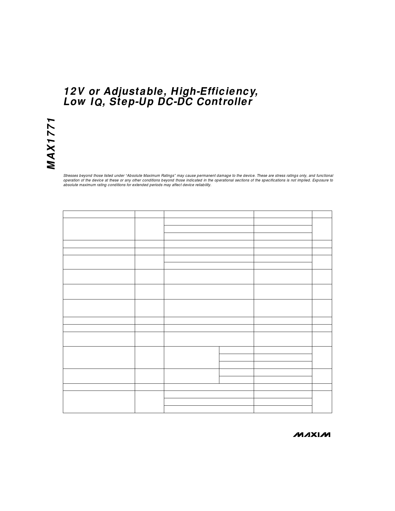
ABSOLUTE MAXIMUM RATINGS
Supply Voltage
V+ to GND ...............................................................-0.3V, 17V
EXT, CS, REF, SHDN, FB to GND ...................-0.3V, (V+ + 0.3V)
GND to AGND.............................................................0.1V, -0.1V
Continuous Power Dissipation (TA = +70°C)
Plastic DIP (derate 9.09mW/°C above +70°C) ............727mW
SO (derate 5.88mW/°C above +70°C) .........................471mW
CERDIP (derate 8.00mW/°C above +70°C) .................640mW
Operating Temperature Ranges
MAX1771C_ A .....................................................0°C to +70°C
MAX1771E_ A ..................................................-40°C to +85°C
MAX1771MJA ................................................-55°C to +125°C
Junction Temperatures
MAX1771C_ A/E_ A.......................................................+150°C
MAX1771MJA ..............................................................+175°C
Storage Temperature Range .............................-65°C to +160°C
Lead Temperature (soldering, 10sec) .............................+300°C
Stresses beyond those listed under “Absolute Maximum Ratings” may cause permanent damage to the device. These are stress ratings only, and functional
operation of the device at these or any other conditions beyond those indicated in the operational sections of the specifications is not implied. Exposure to
absolute maximum rating conditions for extended periods may affect device reliability.
ELECTRICAL CHARACTERISTICS
(V+ = 5V, ILOAD = 0mA, TA = TMIN to TMAX, unless otherwise noted. Typical values are at TA = +25°C.)
PARAMETER
SYMBOL
CONDITIONS
MIN
MAX1771 (internal feedback resistors)
2.0
Input Voltage Range
MAX1771C/E (external resistors)
3.0
MAX1771MJA (external resistors)
3.1
Minimum Start-Up Voltage
Supply Current
V+ = 16.5V, SHDN = 0V (normal operation)
Standby Current
V+ = 10.0V, SHDN ≥ 1.6V (shutdown)
V+ = 16.5V, SHDN ≥ 1.6V (shutdown)
Output Voltage (Note 1)
V+ = 2.0V to 12.0V, over full load range,
Circuit of Figure 2a
11.52
Output Voltage Line Regulation
(Note 2)
V+ = 5V to 7V, VOUT = 12V
ILOAD = 700mA, Circuit of Figure 2a
Output Voltage Load Regulation
(Note 2)
V+ = 6V, VOUT = 12V, ILOAD = 0mA to
500mA, Circuit of Figure 2a
Maximum Switch On-Time
Minimum Switch Off-Time
Efficiency
Reference Voltage
REF Load Regulation
REF Line Regulation
FB Trip Point Voltage
tON(max)
tOFF(min)
VREF
VFB
V+ = 5V, VOUT = 12V, ILOAD = 500mA,
Circuit of Figure 2a
IREF = 0µA
MAX1771C
MAX1771E
MAX1771M
0µA ≤ IREF ≤ 100µA
3V ≤ V+ ≤ 16.5V
MAX1771C
MAX1771E
MAX1771M
MAX1771C/E
MAX1771M
12
1.8
1.4700
1.4625
1.4550
1.4700
1.4625
1.4550
TYP MAX UNITS
12.5
16.5
V
16.5
1.8
2.0
V
85
110
µA
2
5
µA
4
12.0 12.48
V
5
mV/V
20
mV/A
16
20
2.3
2.8
92
1.5 1.5300
1.5 1.5375
1.5 1.5450
4
10
4
15
40
100
1.5 1.5300
1.5 1.5375
1.5 1.5450
µs
µs
%
V
mV
µV/V
V
2 _______________________________________________________________________________________
Share Link: 