A62S7332E-5 데이터 시트보기 (PDF) - AMIC Technology
부품명
상세내역
일치하는 목록
A62S7332E-5
AMIC Technology

A62S7332E-5 Datasheet PDF : 17 Pages
| |||
A63G7332 Series
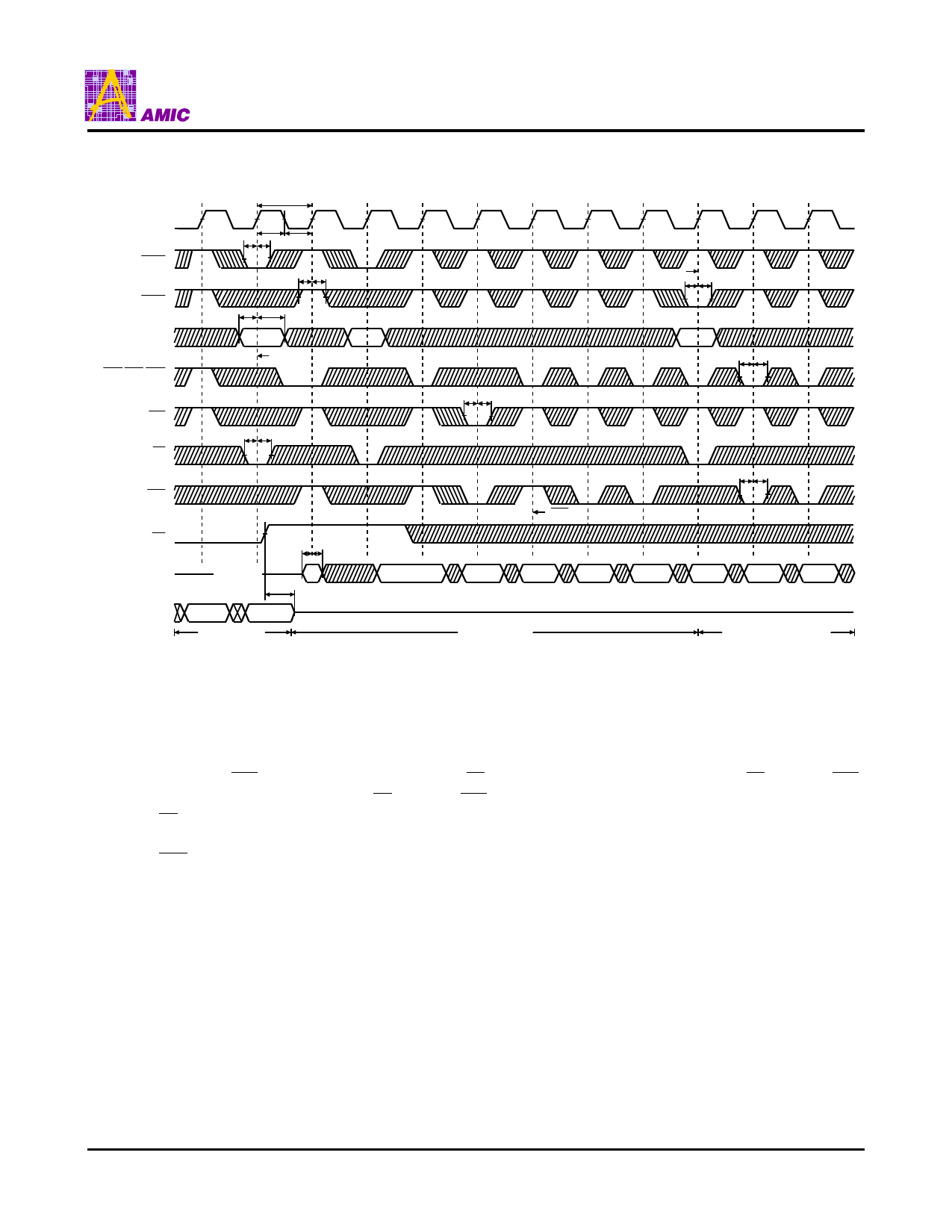
Timing Waveforms (continued)
CLK
ADSP
ADSC
ADDRESS
BWE,BW1-BW4
(NOTE *5)
GW
CE
(NOTE *2)
ADV
OE
DIN
DOUT
tKC
tKH
tKL
tADSS
tADSH
tADSS
tADSH
tAS
tAH
A1
A2
BYTE WRITE signals are ignored
for first cycle when ADSP initiates burst
ADSC extends burst
tADSS
tADSH
A3
tWS
tWH
tWS
tWH
tCES
tCEH
High-Z
(NOTE *3)
tDS
tDH
tOEHZ
D(A1)
(NOTE *4)
ADV suspends burst
tADVS
tADVH
D(A2)
D(A2+1)
(NOTE *1)
D(A2+1)
D(A2+2)
D(A2+3)
D(A3)
D(A3+1)
D(A3+2)
BURST READ
Single WRITE
Extended BURST WRITE
Write Timing
Notes: *1. D(A2) refers to output from address A2. D(A2+1) refers to output from the internal burst address immediately
following A2.
*2. Timing for CE2 and CE2 is identical to that for CE . As shown in the above diagram, when CE is LOW, CE2
is LOW and CE2 is HIGH. When CE is HIGH, CE2 is HIGH and CE2 is LOW.
*3. OE must be HIGH before the input data setup, and held HIGH throughout the data hold period. This prevents
input/output data contention for the period prior to the time Byte Write enable inputs are sampled.
*4. ADV must be HIGH to permit a Write to the loaded address.
*5. Byte Write enables are decided by means of a Write truth table.
PRELIMINARY (December, 1998, Version 2.1)
12
AMIC Technology, Inc.
Share Link: