M74HCT367(1993) 데이터 시트보기 (PDF) - STMicroelectronics
부품명
상세내역
일치하는 목록
M74HCT367
(Rev.:1993)
(Rev.:1993)
STMicroelectronics

M74HCT367 Datasheet PDF : 11 Pages
| |||
M54/M74HCT367/368
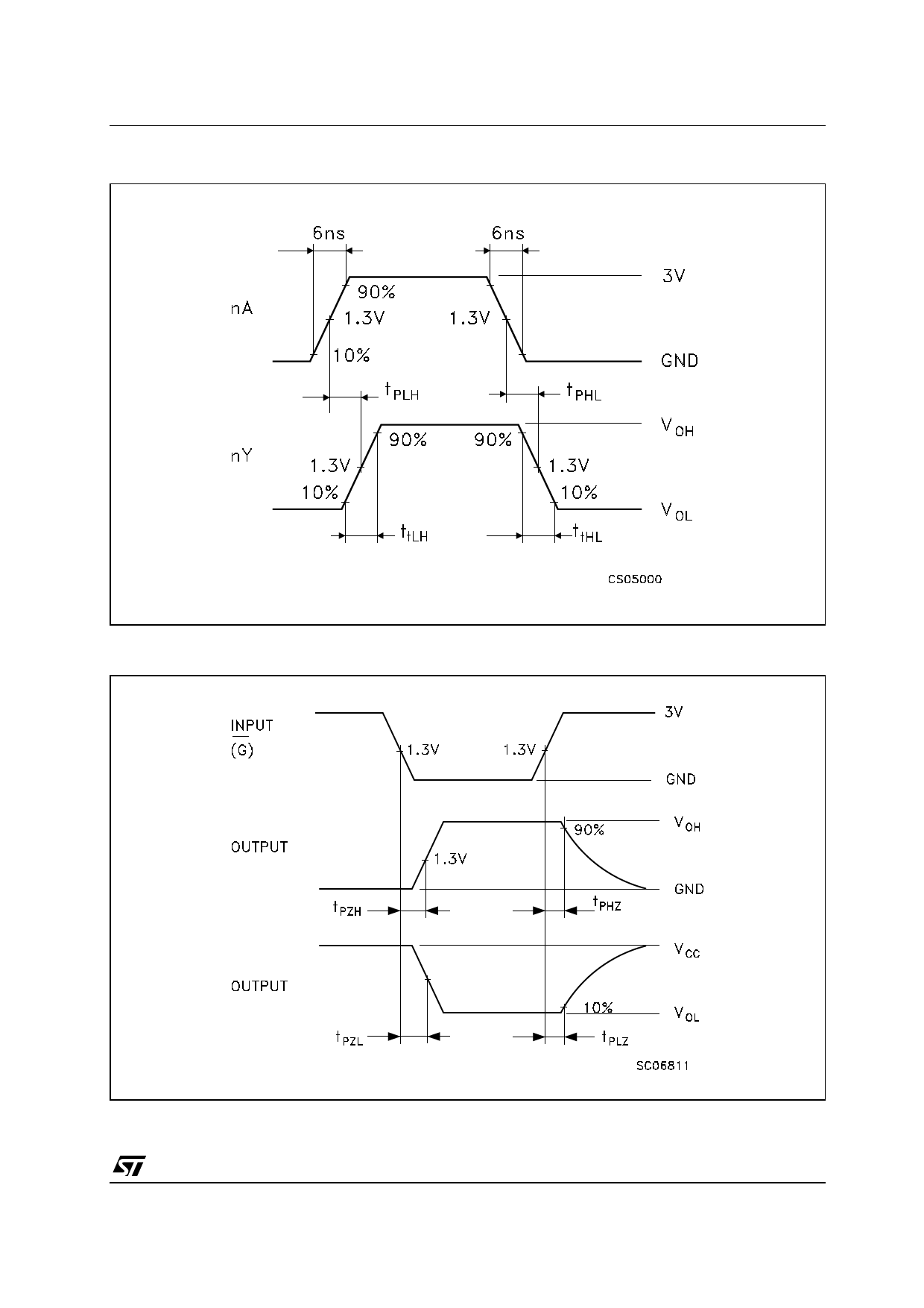
AC ELECTRICAL CHARACTERISTICS (CL = 50 pF, Input tr = tf = 6 ns)
Symbol
Parameter
Test Conditions
VCC CL
(V) (pF)
tTLH Output Transition 2.0 50
tTHL Time
tPLH Propagation
2.0 50
tPHL Delay Time
(for HCT367 only) 2.0 150
TA = 25 oC
54HC and 74HC
Value
-40 to 85 oC -55 to 125 oC Unit
74HC
54HC
Min. Typ. Max. Min. Max. Min. Max.
7
12
15
18
ns
14 22
28
33
ns
18 28
35
42
tPLH Propagation
2.0 50
tPHL Delay Time
(for HCT368 only) 2.0 150
15 24
30
36
ns
19 30
38
45
tPZL Output Enable
tPZH Time
2.0 50
2.0 150
16 25
31
38
ns
20 31
39
47
tPLZ Output Disable
tPHZ Time
2.0 50
18 25
31
38
ns
CIN Input Capacitance
5
10
10
10 pF
CPD (*) Power Dissipation
fot HCT367
47
Capacitance
for HCT368
55
pF
(*) CPD is defined as the value of the IC’s internal equivalent capacitance which is calculated from the operating current consumption without load.
(Refer to Test Circuit). Average operting current can be obtained by the following equation. ICC(opr) = CPD •VCC •fIN + ICC/6 (per Channel)
TEST CIRCUIT ICC (Opr.)
CPD CALCULATION
CPD is to be calculated with the following
formula by using the measured value of
ICC (opr.) in the test circuit opposite.
CPD
=
ICC (opr)
fIN × VCC
In determining the typical value of CPD, a
relatively high frequency of 1 MHz was ap-
plied to fIN, in order to eliminate any error
caused by the quiescent supply current.
* INPUT WAVEFORM IS THE SAME AS THAT IN CASE OF
SWITCHING CHARACTERISTICS TEST.
5/11
Share Link: